MS-8-P-5886 Quantitative HRTEM analysis of epitaxial perovskite multilayer on Si(001) single crystal substrate
Multilayers based on perovskite ferroelectric materials (PbZrxTi1-xO3, BaTiO3, etc.) are intensively studied for the development of ferroelectric random-access memories (FeRAM) or the fabrication of artificial multiferroic devices. High quality epitaxial perovskite multilayers are currently grown by pulsed laser deposition on substrates with perovskite structure and reduced lattice mismatch, like SrTiO3 (STO). The possibility of integrating such perovskite multilayer devices onto silicon chips is of high practical interest. Given the structural difference between Si (diamond cubic structure, aSi= 0.543 nm) and the perovskite layers to be grown on top (pseudocubic lattice parameter ap around 0.39÷0.41 nm), the characterization of the microstructural aspects regarding the growth of the perovskite layers on Si substrates deserves a special attention.
This work contains a quantitative HRTEM analysis of the epitaxial growth of PZT52/48/SrRuO3/SrTiO3 multilayer onto Si(001) substrate. A cross-section specimen has been prepared for TEM by mechanical thinning followed by ion milling at 6o angle of incidence and 4 kV acceleration voltage using a Gatan PIPS installation. The TEM/HRTEM investigation has been performed on a JEM ARM 200F electron microscope operated at 200 kV.
The selected area electron diffraction pattern reveals the epitaxial growth of the STO, SRO and PZT layers. Despite the presence of the amorphous SiO2 layer, there is a clear orientation relationship between the STO layer and the Si substrate: (001)STO || (001)Si and (010)STO || (110)Si.
The mismatch between the (110)Si planes (d110=0.1916 nm) and (010)STO (d010=0.1953 nm) with respect to Si is of 1.9%, considering the bulk values. The pseudocubic lattice constant for the PZT layer measured on the electron diffraction pattern is 0.404 nm, which makes a 3.6% mismatch with respect to the STO lattice parameter. The lattice fringe deformation across the HRTEM micrograph has been analyzed using the Geometrical Phase Method. The HRTEM lattice fringe deformation with respect to (220)Si planes has been mapped out. The numerical values across the map can be read out on the line profile pointing from the substrate to the PZT layer. The measured values of fringe deformation correspond to the bulk values.
Our quantitative HRTEM study indicates that the STO lattice is fully relaxed due to the presence of the amorphous SiO2 layer at the interface, while the PZT layer shows an in-plane compression across the first 10 nm at the interface with the SRO layer. The strained region inside PZT exhibits clusters of dislocations for strain relaxation, as indicated by the geometrical phase image.
The authors acknowledge UEFSCDI and ROSA for financial support through the PN-II-ID-PCE-2012-4-0362, PN-II-ID-PCE-2011-3-0268 and STAR 94/2013 projects.
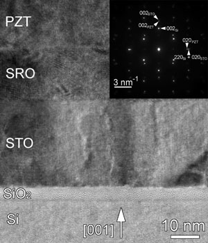
Fig. 1: TEM image displaying the PZT/SRO/STO/Si multilayer structure and the corresponding SAED pattern from a large area including the Si substrate and the deposited multilayer. |
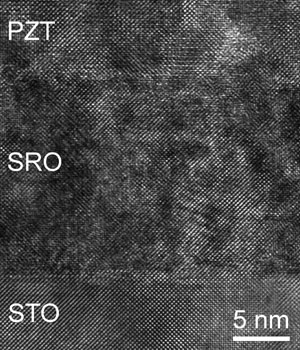
Fig. 2: HRTEM image showing the epitaxial growth of the SRO and PZT layers on the STO layer. |
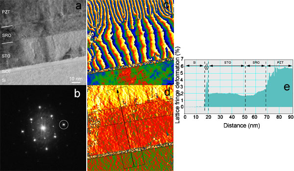
Fig. 3: (a) HRTEM image of the PZT/SRO/STO/Si sample; (b) Corresponding power spectrum; (c) geometrical phase image corresponding to the selected spot 220Si; (d) map of the lattice fringe deformation with respect to the (220)Si lattice planes; (e) averaged line profile of the lattice fringe deformation along the black arrow on map (d). |
|