MS-3-P-3153 TEM characterization of defect free heterostructures grown on a compact home-build molecular beam epitaxy system
Basic Transmission Electron Microscopy (TEM) techniques were used to characterize four period 11 nm InGaAs/10 nm GaAs superlattices, grown on a compact home-build molecular beam epitaxy system. The MBE system, of low investment and low running cost [1], was design to obtain in a small reactor, defect free epitaxial heterostructures, on 10x10 mm substrates. Cross section TEM specimens were prepared along one of the <110> zone axis by mechanical and ion polishing. Compositional, stress sensitive and high-resolution images were obtained using a JEM-3010 microscope, operating at 300 kV, with point resolution of 0.17 nm. Compositional sensitivity dark field images, using the (004) reflection, showed the contrast between the Indium rich and Gallium rich constituents, along the four period superlattice, as seen in Figure 1. The crystallinity quality was observed by dark field, using the (111) reflection (Figure 2), and high-resolution images, which show high quality interface between layers (Figure 3). Dark field images, using the (022) reflection, were also obtained; no defects were observed, rather a strain contrast at the interface due to lattice mismatched between GaAs and InGaAs, as seen in Figure 4. All TEM analysis confirmed the results obtained also by x-ray diffraction (XRD) and atomic force microscopy (AFM), which denote coherent epitaxial growth in the different growth setups of GaAs and InGaAs. All the fundamental growth studies conducted here shown the home-build MBE system produce high quality defect-free InGaAs heterostructures, on GaAs (001) substrates, for optoelectronic applications.
Reference
[1] S. Filipe Covre da Silva, E. M. Lanzoni, P. M. Coelho Neto, A. J. Garcia Jr., A. T. de Barroa, V. Pimentel, C. A. Ospina, J. Bettini, A. Malachias, S. O. Ferreira and Ch. Deneke. Setup and characterization of a compact, home-build molecular beam epitaxy system for overgrowth of small sized substrates. Submitted.
Authors thank M. Cotta, R. M.-Paniago, H. Schuler, F. Huber, K. Eberl, R. Kubiak, FAPESP (2011/22945-1) and CNPq (482729/2013-9), LNLS and LNNano for beamline and TEM facilities.

Fig. 1: Dark Field TEM image, using (004) reflection, sensitive to element concentration, shows four period InGaAs/GaAs superlattice. |

Fig. 2: HRTEM image shows the absence of structural defects by imaging lattice fringes of InGaAs/GaAs. |

Fig. 3: Dark Field TEM image, using (111) reflection, shows high crystal quality (no defects). |
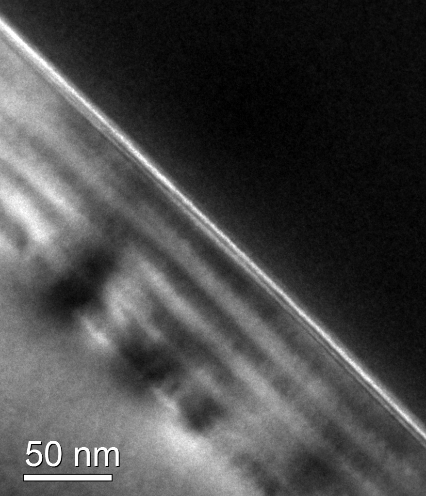
Fig. 4: Dark Field TEM image, using (022) reflection, for strain contrast. |