MS-9-P-3071 HRTEM/STEM characterization of interfaces and strain-related distortions in epitaxial perovskite heterostructures
Most of the currently studied artificial multiferroic systems are based on epitaxial multilayers grown onto SrTiO3 (001) single crystals (STO), using SrRuO3 (SRO) epitaxial layers as bottom electrode. In the ferroelectric heterostructures, the microstructural characteristics of the deposited thin films as well as the interfaces between the ferroelectric layers and the electrodes play a fundamental role in the electrical behavior of the heterojunction (polarization hysteresis loops, C-V and I-V characteristics). Atomic scale structural and chemical characterization plays a major role in further understanding the extrinsic contributions to the electrical characteristics. We have used a Cs probe corrected JEM ARM 200F electron microscope to investigate the interface structure and strain driven structural distortions in the PZT/SRO/STO and BTO/SRO/STO systems, where PZT stands for PbZr0.2Ti0.8O3 and BTO for BaTiO3. Pulsed Laser Deposition (PLD) has been used for the deposition of the epitaxial SRO, PZT and BTO layers onto STO(001) substrates.
We have performed Scanning Transmission Electron Microscopy (STEM) and Electron Energy Loss Spectroscopy (EELS) for the atomic resolution characterization of the SRO-PZT and SRO-BTO interfaces (Figure 1). The atomic interdiffusion at the interface has been studied using the Z contrast in STEM imaging by High-Angle Annular Dark Field and Annular Bright Field. Our studies reveal that an atomic interdiffusion occurs across a region of up to 7 atomic planes around the SRO-PZT and SRO-BTO interfaces. Atomic scale EELS – Spectrum Imaging (EELS-SI) reveals the nature and position of the atomic species at the interface.
SAED patterns from areas including the SRO layer exhibit faint diffraction spots appearing in positions which are not allowed by the reflection conditions in the space groups of SRO, PZT, BTO or STO. FFT of the corresponding HRTEM micrographs prove that the concerned spots are generated from nanometric areas inside the SRO layer. We have performed a quantitative HRTEM study to measure and map the strain fields inside the SRO layer at the nanometric scale. Our study, supported by quantitative image processing by the Geometrical Phase Method and image simulation, clearly proves a strain-driven monoclinic distortion in nanometric domains inside the thin SrRuO3 epitaxial layers, thus explaining the presence of the diffraction spots in forbidden positions in the SAED patterns.
The authors acknowledge UEFSCDI for financial support through the PN-II-ID-PCE-2012-4-0362 and the PN-II-ID-PCE-2011-3-0268 projects.
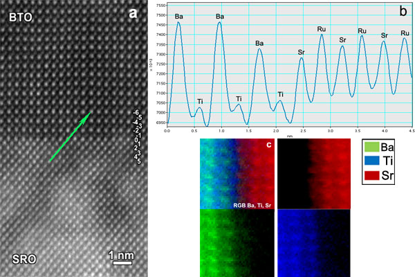
Fig. 1: (a) HAADF – STEM image of SRO - BTO interface; (b) Intensity profile along green arrow through the atomic columns in image (a); (c) Atomic resolution EELS – SI at the SRO - BTO interface. |
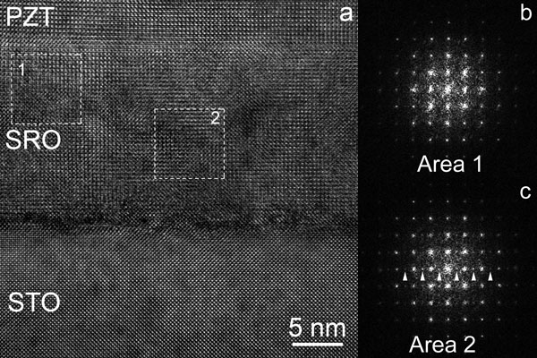
Fig. 2: (a) HRTEM image of an epitaxial SRO thin film sandwiched between the STO(001) substrate and the PZT layer; (b) FFT corresponding to area 1 in HRTEM micrograph; (c) Supplementary spots appearing in the FFT corresponding to area 2 in HRTEM micrograph. |