IT-2-P-2256 STEM Optical Sectioning for Imaging Screw Displacements in Dislocation Core Structures
Aberration corrected transmission electron microscopes have advanced our knowledge of the atomic structure of edge dislocations, which are viewed end-on with the tensile or compressive strain normal to the dislocation being clearly visible. Atomic displacements associated with screw dislocations however cannot be observed end-on because the helical screw displacements are parallel to the viewing direction. In this paper the helical displacements around a screw can be imaged with the dislocation lying transverse to the electron beam by “optical sectioning” in annular dark-field scanning transmission electron microscope imaging. In optical sectioning the few nanometer depth of focus is utilized to extract information along the beam direction by focusing the electron probe at specific depths within the sample. This novel technique is applied to the study of the c-component in the dissociation reaction of a mixed [c+a] dislocation in GaN that has previously been observed end-on [1].
Figure 1 shows atomic layers from different depths of a c-type screw dislocation aligned along the c axis [0001] in GaN. Each layer consists of a (2-1-10) plane, and is parallel to the dislocation line. In layers far from the screw dislocation, the displacements vary slowly across the field of view as expected from the lower shear strain that exists further from the dislocation core. Layers close to the screw dislocation core show displacements that very rapidly in the vicinity of the dislocation core, with a rapidly varying shear of the (0002) planes to given an apparent displacement of c/2 across the dislocation core (as expected for a total Burgers vector of c).
A focal series of experimental images were recorded using a Nion UltraSTEM100 aberration-corrected STEM operating at 100 kV (Figure 2). A 1μm thick sample of GaN, grown by metalorganic vapour phase epitaxy on a sapphire substrate, was thinned to be viewed along the a crystallographic axis. A dislocation was found lying in the plane of the sample, and characterized using weak-beam imaging to be of a mixed [c+a] type along [0001]. As the electron beam is focused closer to the dislocation from (a) to (e), the shearing of the (0002) planes becomes more localized in the image, and a more detailed observation of the screw displacements shows that the shearing occurs equally along two distinct lines along [0001], indicated by the arrows in Figure 2. It is therefore apparent that the screw component of the dislocation has dissociated according to the reaction c=[½ c + ½c] confirming the assumption made in previous end-on observations [1,2].
[1] P.B. Hirsch et al., The dissociation of the [a+c] dislocation in GaN, Philosophical Magazine, 93 (2013) 3925.
[2] H. Yang et al., manuscript in preparation.
The authors would like to acknowledge financial support from the EPSRC (grant number EP/K032518/1) and the EU Seventh Framework Programme: ESTEEM2.
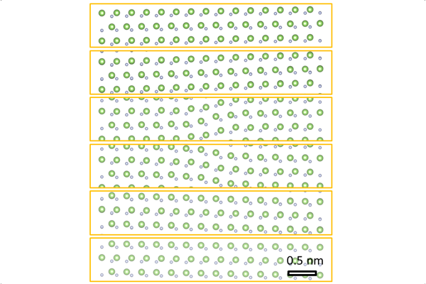
Fig. 1: Figure 1. Structure model of a 10nm thick GaN c type screw dislocation viewed at different depths along direction, with the screw dislocation lying in the middle. From the top to the bottom panel, the distances from the dislocation core are +5, +1, +0.3, -0.3, -1 and -5nm, respectively. |
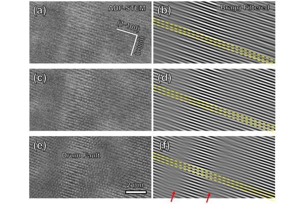
Fig. 2: Figure 2. ADF STEM optical sectioning of a [c+a] dissociated screw dislocation viewed perpendicular to the dislocation line along the a direction. The focal step between (a),(c) and (e) is 4nm. (b,d,f) contain Fourier filtered versions of the corresponding images using just the (0002) Fourier components to highlight the shearing of the planes. |