MS-2-P-1745 Electron microscopic evidence for a tribologically induced phase transformation as the origin of wear in diamond
The origin of wear and the low friction coefficient of diamond is still an intensely debated problem in tribology. Here we study coarse-grained diamond films, deposited by plasma-enhanced chemical vapor deposition, which were tribologically loaded on a ring-on-ring tribometer against a similar diamond counterpart. The microstructure of worn and unworn regions of the diamond film was studied by transmission and scanning electron microscopy. Amorphous carbon (a-C) layers are observed on both as-deposited and on tribologically tested diamond, but differ significantly as far as thickness and morphology are concerned. The a-C layer with a thickness of up to several 100 nm on as-deposited diamond is attributed to the plasma deposition process. For the tribologically tested region of the film, the TEM images (Fig. 1) demonstrate that the µm-sized grains at the rough original diamond surface are almost completely flattened indicating that a significant amount of material must have been removed including the residual a-C layer from the deposition process. In contrast to the as-deposited a-C residue, the tribo-induced a-C layer is comparably uniform with a thickness below 100 nm. The TEM sample from the wear track prepared by conventional techniques (Fig. 2) confirms the findings of the FIB-prepared sample. A few of the TEM samples containing a tribo-induced a-C layer contain grain boundaries of the underlying polycrystalline diamond in the electron transparent region. It is found that the thickness of the a-C layer changes quite abruptly on grains with different crystallographic orientations (white arrow in Fig. 2). Fig. 3 clearly shows that the interface between the crystalline diamond and the tribo-induced amorphous a-C layer is not crystallographically flat but displays a nm-scale roughness. The anisotropic phase transformation and the small roughness of the interface are regarded as evidence for an atom-by-atom wear process. Quantitative electron energy loss spectroscopy of the C-K ionization edge, performed in a transmission electron microscope, reveals the transition from sp3-hybridized C-atoms in diamond to a high fraction (65 %) of sp2-hybridized C-atoms in the tribo-induced a-C layer within a region of less than 5 nm thickness.
XZ acknowledges funding from China Scholarship Council (CSC) (No. 2010606030). PG acknowledges support from Deutsche Forschungsgemeinschaft DFG (project grant Gu 367/30).
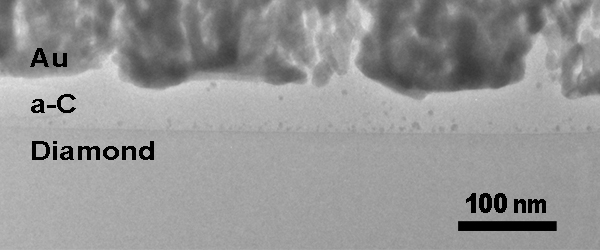
Fig. 1: Overview TEM image of a cross-section FIB-lamella taken from the wear-track region. |
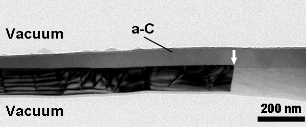
Fig. 2: Overview TEM image of a conventional cross-section TEM sample prepared from the wear-track region. |
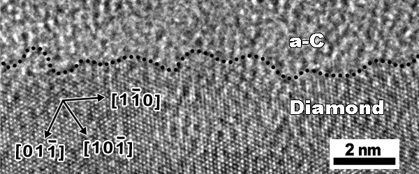
Fig. 3: HRTEM image of the interface region between crystalline diamond and the tribo-induced amorphous carbon layer with the diamond oriented along the [111] zone axis. The approximate position of the interface is marked by a dashed line. |
|