IFSM-PL-6100 From the Prague Spring to a Spring in Electron Microscopy
Prague is my native city: I was born in Praha-Bubeneč, on the plateau behind the Prague Castle. I grew up in the era of the Czechoslovak Socialist Republic (ČSSR), when the Soviet Union and its satellites prided themselves on their space exploits and their education systems. Among the special efforts they made were competitions for talented youngsters in mathematics and physics, and I used to enjoy those. In my senior high school year, I qualified for the national round in both math and physics, and in physics I was invited onto the national team of three that represented Czechoslovakia at the 2nd International Physics Olympiad, held in Budapest in June 1968. Back then only the Soviet Union and its satellites participated – Western Europe, USA and other countries joined the Physics Olympiad later. Our team did well: we got a joint second place with the Hungarians and the East Germans, with the Soviets winning the first place. I have since then had the pleasure of working with one other former International Physics Olympian – Niklas Dellby, my partner at Nion.
That same summer I took the entrance exam to Charles University in Prague, to study physics. I passed and promptly took off on a trip I had planned: a vacation in the south of France, followed by a stay in London where I was planning to work in a summer job while improving my English. 1968 was the year of the famous Prague Spring, when “socialism with a human face,” which included many democratic measures, was introduced by a group of reformers led by Alexander Dubček (Fig. 1a), much to the displeasure of the old guard in the Kremlin. As I was boarding the train to France, my father told me: “If the Soviets invade, stay in the West.” I had not been following the political situation very closely, so this came as a surprise instruction to me. The Soviets invaded 4 weeks later (Fig. 1b), while my whole family happened to be in the West: my parents on vacation in Austria, my sister working in a summer job in France and me working as an office helper in London. We got together on the phone, and decided that none of us would go back to Prague, at least not for the time being. (See [1] for an especially lucid account of the Prague Spring.)
People were very sympathetic to citizens of a small country invaded by Soviet tanks, and the British National Union of Students had a special place in its London office for notices of available openings for prospective Czech and Slovak students. I was checking it daily while working in a new job, as a carpenter. Around the end of September, a small notice appeared, announcing that the University of Leeds was going to offer up to 5 scholarships to qualified Czechoslovak students. I called them up and caught the train to Leeds soon thereafter. There was an entrance interview during which it became clear that I knew my physics all right, and also that 3 years of high school English and a vocabulary of perhaps 3000 English words were not nearly enough for me to slot painlessly into the British university system.
Leeds took a chance on me, and at first they must have wondered how it would turn out. In my first year I got a First in math – understanding equations did not require much English – but only a Pass in physics, in which there were long textbook passages that I studied laboriously, with a dictionary in hand. I did better in later years, graduating with a First, at the top of my class. I was then accepted to do a physics Ph.D. in Cambridge, with Archie Howie as my inspiring supervisor. In my first year, our lab was not far from Ellis Cosslett’s, after whom the award I received is named, and who has been one of my heroes in electron microscopy, especially after I came to appreciate the pioneering nature of much of the work of his group.
I greatly enjoyed my time in Cambridge, both inside and outside the Physics Department. I learned a lot, made many friends, and made good use of Cambridge’s excellent extra-curricular facilities. I raced for Cambridge against Oxford in skiing and won the special and parallel slaloms at the 1975 Oxford-Cambridge ski race, in the Italian Dolomites. The 8-man boat crew I joined the previous spring (Fig. 2) did three bumps and an overbump in the Cambridge May Races, and by Cambridge tradition, we got to keep our oars as souvenirs.
After Cambridge, I worked at Kyoto University for 3 months, and did post-docs at Bell Labs and UC Berkeley, where I joined the group of Gareth Thomas in the Materials Science Department. Being in Materials Science made me feel that I had to make a choice: I could concentrate on the materials we were studying and become a materials scientist, or on the instruments and techniques we were using and remain a physicist. I had done a little instrument design work and liked it, so the second option seemed more attractive. The technique I thought was especially interesting was a new one (to me) called Electron Energy Loss Spectroscopy (EELS). I got my first taste of it at the 1978 Cornell workshop, where I met people who became lifelong friends, such as Phil Batson, Christian Colliex, Ray Egerton, and Mike Isaacson. One was expected to build one’s own spectrometer in those days – there were no commercial models. When I got back to Berkeley, I climbed the stairs to Professor Thomas’s office and said: “I think I should build an energy loss spectrometer. It will allow us to study oxygen concentrations at grain boundaries in nitrogen ceramics.” – a subject the group was focusing on. Gareth asked just one question: “How much will it cost? ”, I replied “about $10k”, and I had my first OK to build a major instrument.
The spectrometer came together quickly and produced good results (Fig. 3). In the summer and autumn of 1979, I was showing the results at various conferences. At one of them, at NBS in Washington, Nancy Tighe came up to me and said: “I think your spectrometer would interest Peter Swann of Gatan. You should give him a call.” This started my fruitful collaboration with Peter, from whom I learned on many fronts. Peter passed away in the summer of 2013, and many of us miss him very much.
Over the next year, Peter Swann, Joe Lebiedzik and I, with input from Mike Scheinfein, designed and built a second-generation serial EEL spectrometer. I also started in a new job, as Associate Director of the NSF-funded HREM facility at Arizona State University. With my collaborators at ASU, we applied the spectrometer to many interesting problems, and put together the EELS Atlas [2] that is used to this day. ASU was a great place to work. There were many good instruments, several leading researchers in electron microscopy, and stimulating annual schools and workshops (Fig. 4), whose organization was my responsibility.
The pull of Gatan, however, proved irresistible when Peter moved its R&D facility from Pittsburgh to California, and in 1985 I became Director of Research at Gatan. A very productive period followed, during which I had the privilege of working with many talented researchers and designers: Dan Bui, Niklas Dellby, Garry Fan, Stuart Friedmann, Sander Gubbens (the current President of Gatan), Robert Keeney, Bernd Kraus, Mike Kundmann, Mike Leber, Chris Meyer, Paul Mooney, Ming Pan, Nils Swann, Peter Swann, Marcel Tence and Jacob Wilbrink, among others. We introduced a number of innovative products, including parallel EELS, imaging filters, CCD cameras, scanned image acquisition systems and DigitalMicrograph software. Gatan grew nearly 10x in size during this time, and I learned that developing instruments commercially can be a great way to fund instrumentation research, especially when working with like-minded researchers and lean and understanding administrations.
The next big change in my scientific life came when Peter decided to retire in 1992, and “professional managers” took over at Gatan. My freedom to do interesting projects was greatly restricted, and I started to look around. It had been clear to me since about 1990 that having managed to correct the second order aberrations of the quadrupole optics of imaging filters, I had a good chance of correcting third order aberrations – a classic problem in electron optics since Scherzer’s work on the subject in the 1930s and 40s. It seemed too speculative a project for Gatan, however, and so I explored doing it elsewhere. My first try for corrector funding was a chat with Uli Dahmen, the Berkeley NCEM director, who consulted with Bob Gottschall, his manager at DOE. Bob’s answer was apparently “over my dead body.” He had gotten burned funding Crewe’s corrector attempts, which never led to a working instrument.
I was more successful persuading Mick Brown of my Alma Mater, Cambridge University, who had a spare VG cold field emission (CFE) scanning transmission electron microscope (STEM), that we should jointly build a corrector for it. We applied for funding to the British Royal Society and secured the maximum allowed amount from the Paul Instrument Fund: £80k. I then moved to Cambridge with my family for two wonderful years. Niklas Dellby and others joined the project, and we had a working proof-of-principle STEM corrector about 2 years later [3], the same summer (1997) as the Heidelberg-Julich CTEM corrector started working.
The 100 kV VG STEM we built our corrector for was older than a research student who joined the project (Andy Lupini), and it had poor aberration coefficients (Cs~Cc~3.5 mm). We improved its resolution, but we did not beat any resolution records relative to the best uncorrected instruments. (The same was true for the Heidelberg effort – 1 MV microscopes were then giving higher resolution than their corrected 200 kV CTEM.) However, a corrector of an improved design we built for Phil Batson’s extensively modified VG at IBM Yorktown Heights achieved a double distinction: it led to the first STEM able to focus an electron probe to <1 Å diameter [4], and it was, as far as I know, the first commercial corrector (delivered in June 2000).
Aberration correction soon became a “hit”, with CEOS GmbH supplying correctors to all the regular manufacturers of electron microscopes, and the company Niklas Dellby and I started near Seattle, Nion, concentrating on correctors for CFE STEM and going it alone. Our idea was a somewhat crazy one: that we could extend our prowess in correctors by designing a whole new electron microscope, and that we would do it better than the regular manufacturers. Not many thought that we would succeed. But there were early believers to whom we owe a great deal, such as John Silcox, Andrew Bleloch, Steve Pennycook and Christian Colliex. Benchmarks established subsequently by Nion for resolution, stability, probe current, ultra-high vacuum, freedom from contamination and powerful software [5,6] have persuaded many others.
Nion’s very capable team - Niklas Dellby, Neil Bacon, George Corbin, Peggy Cramer, Zeno Dellby, Russ Hayner, Petr Hrncirik, Tracy Lovejoy, Chris Meyer, Savath Phoungphidok, Michael Sarahan, Gwyn Skone, Zoltan Szilagyi, Janet Willis, Tad Yoo and myself for now, and growing, has done some amazing things. We first delivered 10 aberration correctors for VGs, then moved onto making whole electron microscopes. Currently we’re manufacturing Nion microscopes #10-13, and the interest in our instruments is on the rise. Building the instruments has been made easier by the close collaboration we enjoy with Czech Republic’s Delong Instruments, especially Vladimír Kolařík and Petr Homolka. Nion’s progress has also been helped by two simple facts: ordering an electron microscope from a small company is a gutsy thing to do, and gutsy scientists tend to be first-rate. (Figs 5-7) and references [7-13] show some of the revolutionary results they and their collaborators have obtained with Nion microscopes.
Aberration correction has ushered in an era of electron microscopy in which we can see the structure, composition and bonding of materials better than ever before. It amounts to a new spring in electron microscopy, best captured by the words of David Cockayne: “it is as though a veil of fog has lifted from our samples.” It is about to get better still, because of an exciting new development: studying energy losses with sub-20 meV energy resolution and sub-nm spatial resolution. This has been made possible by Nion’s new monochromator [14], which has been the subject of two separate talks at this congress [15], and which promises to make vibrational excitations in materials (phonons) readily observable (Fig. 8), at a high spatial resolution. It will probably also allow hydrogen to be mapped in the electron microscope, using energy losses that accompany high-angle scattering of fast electrons by hydrogen nuclei.
My scientific instrumentation journey began with EELS and progressed onto aberration correction and high resolution STEM. It has now come back to EELS, with an energy resolution about 100x better than on my first try. My life’s journey began in Prague, and Prague is where this congress has been held. Both journeys are reminiscent of the famous lines by T.S. Eliot [16]:
We shall not cease from exploration,
And the end of all our exploring
Will be to arrive where we started
And know the place for the first time.
So let us celebrate exploration (also known as research) and knowing where we came from. And also congresses such as IMC, which enrich our knowledge of our field, and of ourselves.
[1] A. Levy, Rowboat to Prague (ISBN 0-670-60920-X), reprinted as So Many Heroes (ISBN 978-0933256125). See also http://en.wikipedia.org/wiki/Alan_Levy
[2] C.C. Ahn and O.L. Krivanek, EELS Atlas (1983) Gatan and the ASU HREM facility.
[3] O.L. Krivanek et al., Proc. EMAG 1997, IOP Conf. Ser. No 153 (J. Rodenburg, ed.) 35-40.
[4] P.E. Batson, N. Dellby and O.L. Krivanek, Nature 418 (2002) 617-620.
[5] O.L. Krivanek, et al., Ultramicroscopy 108 (2008) 179-195.
[6] N. Dellby et al., The European Physical Journal Applied Physics 54 (2011) 33505 (11 pages).
[7] D.A. Muller et al., Science 319 (2008) 1073-1076.
[8] O.L. Krivanek et al., Nature 464 (2010) 571-574.
[9] T.C. Lovejoy et al., Appl. Phys. Letts 100 (2012) 154101 to 154101-4.
[10] P.Y. Huang et al., Nano Letters 12 (2012) 1081-1086.
[11] W. Zhou et al., Microscopy and Microanalysis 18 (2012) 1342-1354.
[12] Q.M. Ramasse et al., Nano Letters 13 (2013), 4989–4995.
[13] J. Lee at al., Nature communications 4 (2013) 1650.
[14] O.L. Krivanek et al., Microscopy 62 (2013) 3-21.
[15] N. Dellby et al., these proceedings and O.L. Krivanek et al., these proceedings.
[16] T.S. Elliot, Four Quartets (1943) ISBN 978-0156332255.
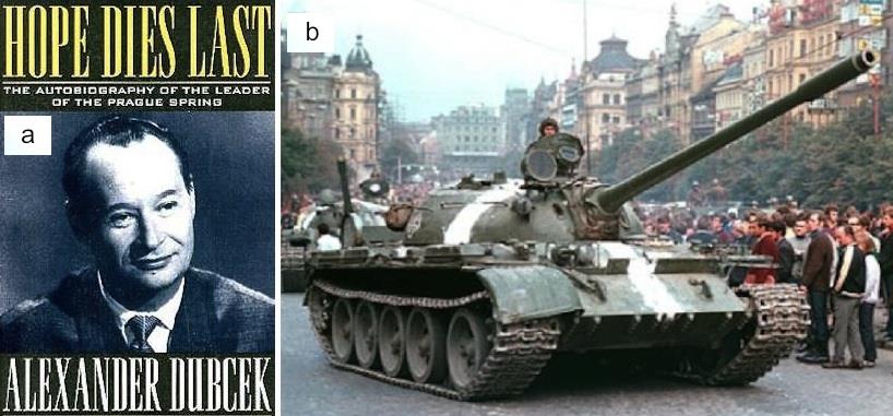
Fig. 1: a) Alexander Dubček, who led the Prague Spring. b) Soviets tanks rolling through Prague’s Wenceslas square. |
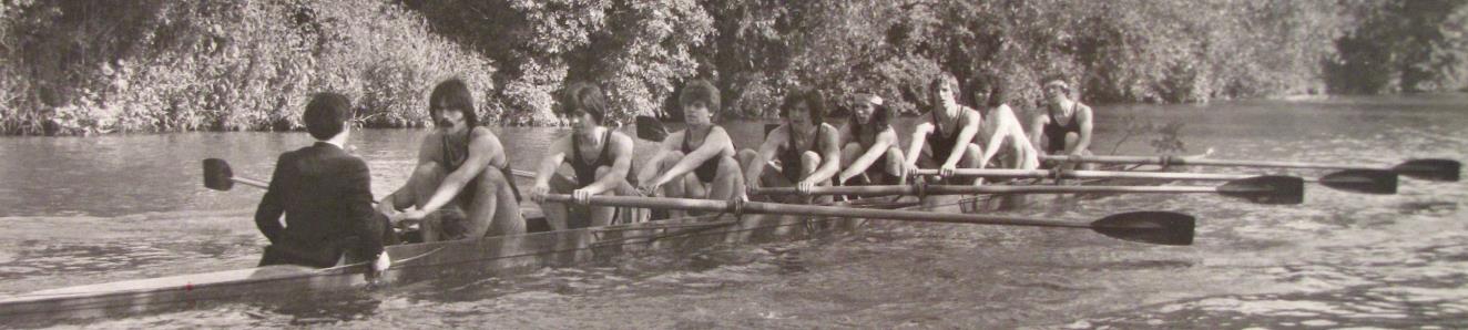
Fig. 2: Rowing on the river Cam. I am in seat #5 (bow = 1), holding the oar that does not quite match the others. d) 1981 ASU meeting. Front row: Mike Isaacson, Alan Craven, John Spence, John Venables, Albert Crewe, John Cowley, Bernard Jouffrey, Ian Wardell, Ondrej Krivanek, Colin Humphreys. Spot Ray Carpenter, Mark Disko, Murray Gibson, Sumio Iijima, Kazuo Ishizuka, Masashi Iwatsuki, Charlie Lyman, Peggy Mochel, Steve Pennycook, Jing Zhu and others in the photo. |
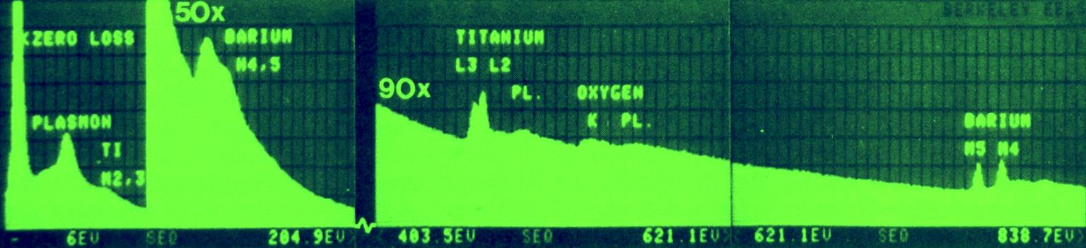
Fig. 3: EEL spectrum of BaTiO3 recorded with the serial EEL spectrometer I built at Berkeley, at about 2 eV resolution. 1981 ASU meeting. Front row: Mike Isaacson, Alan Craven, John Spence, John Venables, Albert Crewe, John Cowley, Bernard Jouffrey, Ian Wardell, Ondrej Krivanek, Colin Humphreys. Spot Ray Carpenter, Mark Disko, Murray Gibson, Sumio Iijima, Kazuo Ishizuka, Masashi Iwatsuki, Charlie Lyman, Peggy Mochel, Steve Pennycook, Jing Zhu and others in the photo. |
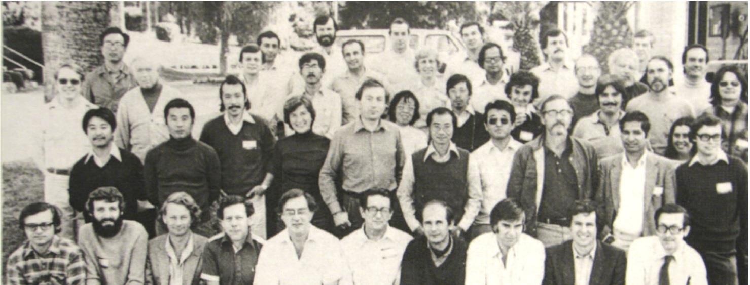
Fig. 4: 1981 ASU meeting. Front row: Mike Isaacson, Alan Craven, John Spence, John Venables, Albert Crewe, John Cowley, Bernard Jouffrey, Ian Wardell, Ondrej Krivanek, Colin Humphreys. Spot Ray Carpenter, Mark Disko, Murray Gibson, Sumio Iijima, Kazuo Ishizuka, Masashi Iwatsuki, Charlie Lyman, Peggy Mochel, Steve Pennycook, Jing Zhu and others in the photo. |
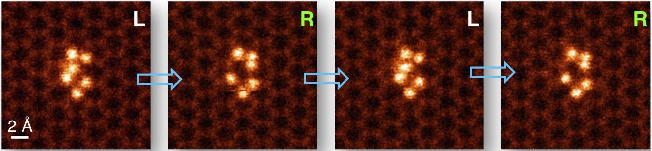
Fig. 5: Reversible atomic motion in monolayer graphene: one of the 6 substitutional Si atoms moves right, left, right. Nion UltraSTEM100, 60 kV, 6 s between frames. (Ref. [13]) |
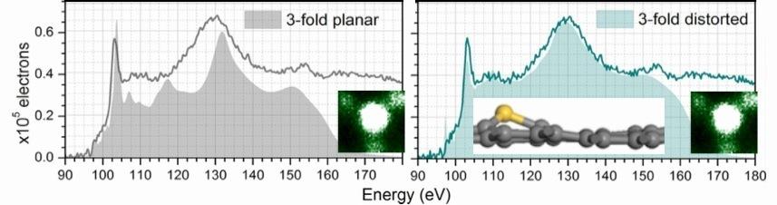
Fig. 6: EEL L2,3 spectrum from a single Si atom replacing a C atom in graphene (line) and theoretical fits (solid spectra). The right fit allowed the Si atom to “pop out” 0.65 Å from the graphene plane (inset) and gave better agreement. (Ref. [12]) |
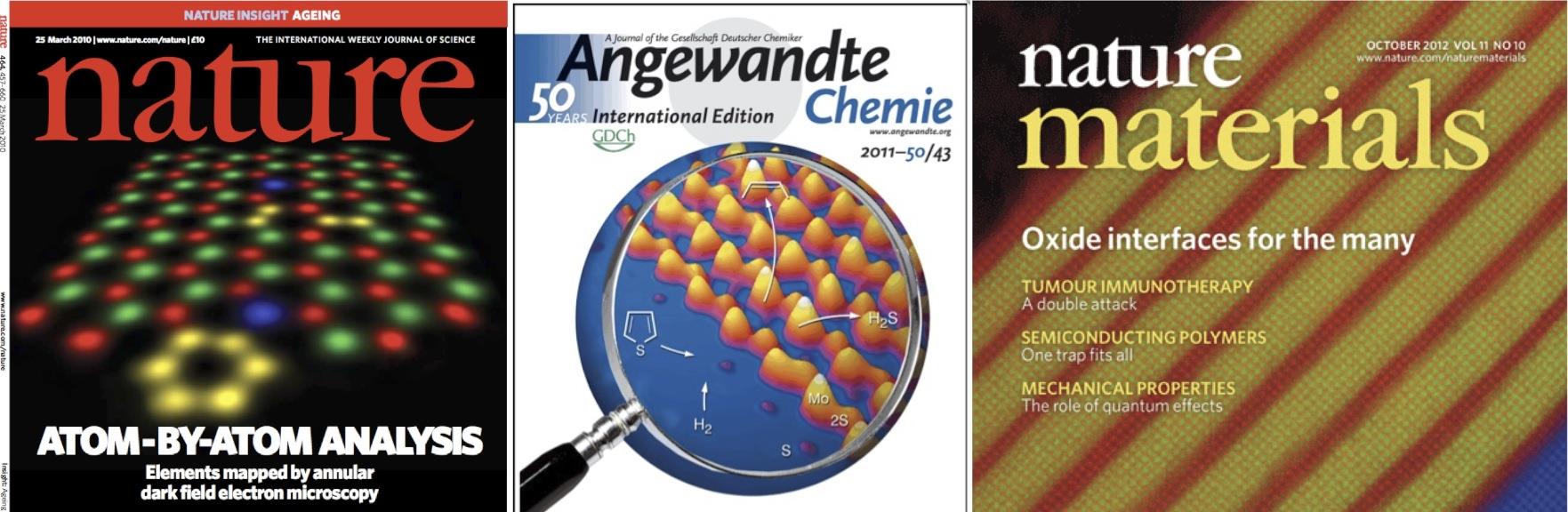
Fig. 7: Results from Nion microscopes. Nature vol. 464 (2010) issue 7288 cover: image of BN monolayer with impurities by Matt Chisholm, processing by the author and Tim Pennycook. Angewandte Chemie vol. 50 (2011) issue 43 cover: image of MoS2 by Quentin Ramasse. Nature Materials vol. 11 (2012) issue 10 cover: EELS elemental map by Julia Mundy. |
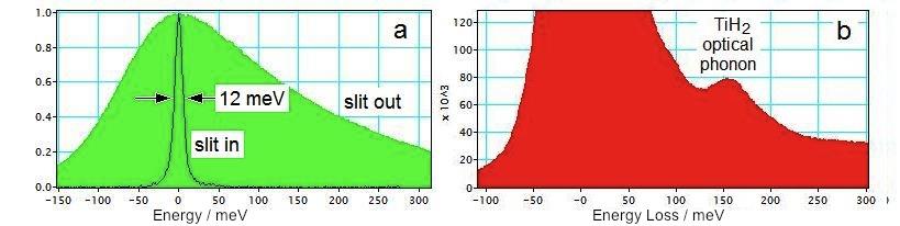
Fig. 8: 60 kV results from the Nion High Energy Resolution Monochromated EELS-STEM (HERMES). a) Spectra obtained with the slit out and in, slit-in acquisition time 0.25 s, courtesy Niklas Dellby (Nion) and Philip Batson (Rutgers U.). b) spectrum from titanium hydride (acq. time 10 s), courtesy Peter Crozier and Jiangtao Zhu (ASU), and Tracy Lovejoy (Nion). |