IMC-PL-6098 Electron Tomography for Nanoscale Materials Science
The nanoscale complexity of modern materials and devices, be they structural or functional in design, requires high spatial resolution characterisation in all 3 dimensions. The remarkable power and flexibility of a modern TEM makes it the ideal tool for such 3D nanoscale imaging and analysis. Over the past 15 years or so, electron tomography (3D imaging) has grown from a niche technique to one which is now firmly established as an almost routine tool for the 3D study of materials. Early electron tomography used many of the ideas and practices established first in the life sciences. Here, a tilt series of bright-field (BF) images are acquired by rotating the sample about a single axis and recording images every 1-2°. Typically, in the electron microscope, the range of sample tilt is limited either by the sample itself (becoming too thick) or by the objective lens pole piece gap. As such, it is therefore likely that the full tilt range is not accessible, this leads to a ‘missing wedge’ of information and the reconstructions suffer from artefacts, especially an elongation parallel to the optic axis. Dual axis tomography can help in this regard, reducing the missing information through a second tilt series about an axis mutually perpendicular to the first.
For many materials problems, however, BF images may not be ideal and the introduction of STEM HAADF tomography offered materials microscopists an imaging mode that, in many cases, is much more suited for tomography, providing images with greatly reduced diffraction contrast, with a signal that in most cases varies monotonically with thickness (satisfying the projection requirement) and providing compositional contrast through the atomic number (Z) dependence of the high angle (Rutherford-like) scattering [1]. STEM tomography has now become for many the technique of choice for 3D nanoscale imaging in materials science. Fig. 1 shows two examples of STEM HAADF tomography [2,3]. In Fig. 1(a) we see Ge precipitates within an Al-rich matrix revealing a wide variety of morphologies and clear orientation relationships and in (b) the 3D distribution of Ru-Pt catalyst nanoparticles (1-2nm in size) decorating the surface of a mesoporous silica support – here we see only the external surface. The colour of the support indicates the surface curvature with a strong preference of the nanoparticles to be anchored at the ‘saddle points’. STEM tomography (both BF and ADF) has also been developed for the study of defects (especially dislocations) where the reconstruction (or 3D representation) of the dislocation resembles a ‘string’ running through space.
Although determination of the 3D morphology of materials at the nanoscale is now essentially routine, to achieve a high fidelity reconstruction typically ca. 100 images are needed across the tilt range. For many specimens long acquisition times, and thus extended exposure, can lead to damage. However, the number of images required in the tilt series can be reduced if there is prior knowledge about the specimen being reconstructed. Such prior knowledge can be used within a discrete tomography reconstruction (using the physical discreteness of the sample) or, perhaps more generally, within a compressed sensing framework where the primary requirement is that the sample may be described as being ‘sparse’ in some transform domain [4,5]. This sparsity constraint turns out to be very powerful and high fidelity reconstructions can be achieved with remarkably few images (in some cases an order of magnitude reduction compared to conventional reconstructions), see Fig. 2.
Coupling tomography acquisition with analytical techniques, such as EDX and EELS, allows a more detailed exploration of the sample’s chemistry as well as its morphology. Early efforts in this direction included the use of EFTEM, especially using the low loss regime (where loss probability is relatively high), EDX and core-loss EELS. Inevitably, although the speed and efficiency of spectrometers has improved greatly over the past few years, the acquisition time needed for multi-dimensional ‘spectrum-images’ is considerably higher than a conventional image. To keep the total exposure to a reasonable level, fewer images are recorded in the tilt series – ideally perhaps only every 10 or 20°. The reduction in data must be compensated by an increase in prior knowledge to achieve a high fidelity reconstruction; for such ‘multi-dimensional microscopy’ [6], compressed sensing offers an important framework to achieve this. As an example, Fig. 3(a) shows a composite figure illustrating the localised surface plasmon resonances from a silver nanocube. The reconstruction was undertaken on a series of spectrum-images recorded about a single tilt axis every 15°. The 4mm symmetry of the cube-substrate system was imposed at the reconstruction stage as well as a constraint that the reconstruction could be considered as being sparse in a wavelet domain. That constraint provided a reconstruction relatively free of artefact even when using few images [7]. Interpretation of the reconstruction seen in Fig.3(a) can be made within a quasi-static approximation and related back to the potential induced by the electron beam acting back on the electron. Mapping electro-magnetic potentials is also possible using electron holography and coupled with tomography was able to yield 3D reconstructions of the built-in potential near a p-n junction in a silicon device, see Fig. 3(b) [8]. 3D magnetic fields require an enhanced approach using dual axis geometry to determine all the components of the magnetic potential A (or induction B). Here, physical constraints (e.g. in the form of Maxwell’s equations), perhaps again within a compressed sensing framework, could be used to improve a reconstruction of the electro-magnetic potential.
So, what of the future? The electron tomography community is pushing in many directions. Atomic resolution tomography has been demonstrated in some cases: by assuming periodicity within a nanocrystal, the position of an isolated atom in a matrix can be determined and even the location of atoms around a dislocation core. Synergisitc studies with atom probe tomography have been demonstrated already and this may, in the future, develop into an important correlative approach. Mapping physical properties in 3D at the nanoscale continues to be an exciting prospect. Whilst early work showed this to be feasible, further development is needed to improve reconstruction quality. Given the almost ubiquitous use now, in materials-based tomography at least, of iterative techniques (e.g. SIRT, ART, etc) the conventional projection / back-projection approach could evolve into a more model-based one incorporating a detailed description of the beam’s interaction with the sample along its trajectory (e.g. dynamical effects). By iteratively refining an initial model, increased detail about the sample may be obtainable (e.g. strain, fields, induced charges). Lastly, industry requires a robust nanoscale metrology technique that provides reliable 3D measurements of length, porosity, distributions etc. We are still some way in many cases of being able to provide such data with statistical confidence (i.e. error bars!) on our 3D measurements. Improved reconstructions, with fewer artefacts, incorporating prior knowledge, should allow improved and unbiassed segmentation and thus will go a long way to providing a true 3D nanometrology technique.
References:
[1] P.A. Midgley et al., Chem. Commun. (2001) 907
[2] K. Kaneko et al., Ultramicroscopy 108 (2008) 210
[3] E.P.W. Ward et al., J. Phys. Chem. C 111 (2007) 11501
[4] Z. Saghi et al., Nano Letters 11 (2011) 4666
[5] R. Leary et al., Ultramicroscopy 2013 131 70-91
[6] P.A. Midgley and J.M. Thomas, Angewandte Chemie (2014) DOI: 10.1002/anie.201400625
[7] O. Nicoletti et al., Nature 502 (2013) 80
[8] A. Twitchett-Harrison et al., Nano Letters 7 (2007) 2020
The author thanks his many colleagues, past and present, who have contributed to the work presented here including most recently J.M. Thomas, R. Leary, Z. Saghi, D. Holland, K. Kaneko, S. Hata, O. Nicoletti, F. de la Peña, C. Ducati. PAM acknowledges funding from the European Research Council under FP7/2007-2013 / ERC grant agreement 291522-3DIMAGE.
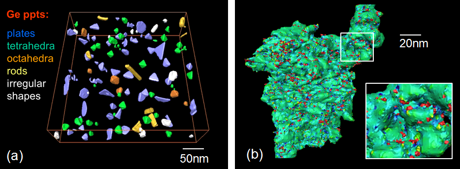
Fig. 1: (a) 3D reconstruction of Ge precipitates in an Al-rich matrix showing colour-coded to highlight theor different morpholgy [2]; (b) Ru-Pt catalyst particles (red) shown on a colour-coded silica surface where the blue regions indicate positive Gaussian curvature (saddle points) [3]. |
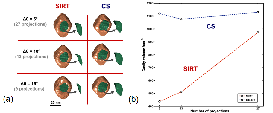
Fig. 2: (a) Comparison of reconstructions using SIRT and compressed sensing (CS) codes for an iron oxide nanoparticle with a concavity; (b) the apparent concavity volume as a function of projection number [4]. |
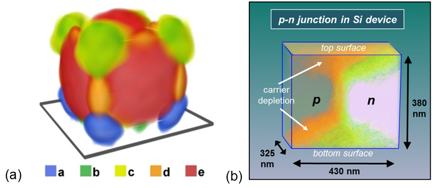
Fig. 3: (a) Colour composite figure indicating five surface plasmon modes on a silver nanoparticle, 100nm in size [7]; (b) Reconstructed electrostatic potential near a p-n junction in a silicon device showing sub-surface carrier depletion [8]. |
|