IMC-PL-6097 Imaging and Spectroscopy of Individual Atoms in Nanostructured Materials
It has remained a challenge for scientists to image and discriminate individual atoms since Dalton first proposed distinct properties of atoms in his atomic theory. The requirements to analyze the atomic structures of matter with elemental information are nowadays increasing in importance of cutting-edge research. An elemental analysis down to the single atom limit was first demonstrated with the successful detection of a Gd dopant atom in carbon nano-peapods using a STEM-EELS technique at 100kV [1]. Specimen damage due to the high dose of the incident electron beam, which is required to isolate the signals from individual atoms, is an intrinsic problem for such a highly delicate analysis. Furthermore it is important to prevent the atoms from being kicked out during the observations. In order to reduce the atomic movements and also to enhance the EELS contrast, a lower accelerating voltage is preferred for single atom detection by STEM. Sawada et al. designed a new type of aberration corrector with triple dodecapole elements (the delta system) to reduce the higher-order geometric astigmatism [2, 3, 4], which is critical for the STEM performance operated at low accelerating voltages, i.e., 15 to 60 kV. Here, I demonstrate successful single-atom imaging and spectroscopy in nanostructured materials using STEM together with EELS and/or EDX.
Fig. 1 shows an example for chemical analysis of individual molecules. A carbon nanotube encapsulating two different metallofullerenes (La@C82 and Ce@C82) is examined at 30 kV operating voltage [5]. The annular dark-field (ADF) image clearly shows the molecular structures encapsulated inside the SWNTs (Fig. 1a). Each molecule carries one metal atom, appearing in brighter contrast, inside the cage. We can identify these atoms by simultaneous EELS. Fig. 1b shows two EELS spectra recorded from two atoms. The EELS spectrum shown in green corresponds to the atom indicated by the green arrow. This spectrum is the sum of four spectra, each of which had an acquisition time of 0.05 s. The resulting signal-to-noise ratio is high enough to isolate the La N-edge. On the other hand, the atom indicated by the blue arrow is assigned as Ce. Moreover, its peak position (≈122 eV) fits very well with that for Ce3+ [6]. Though the two edges of La N and Ce N overlap severely, we could identify the elements (La: Z = 57 and Ce: Z = 58) comprising the two encaged atoms. Fig. 1c shows the ADF image, and the elemental mappings for La, Ce, and carbon are shown in Figs. 1d, e, and f, respectively. A further comparison of simultaneous EELS and EDX measurement allows us to directly estimate the fluorescent yield of single atoms [7, 8].
The interrupted periodicities of 2D materials such as graphene, h-BN, and MX2 (dichalcogenides) are of great interest because they govern the physical/chemical properties. Atomic defects, such as a vacancy or impurity/dopant in single-layered materials are investigated with atomic precision. A single-layer of MoS2 exhibits interesting physical properties. The electrical conductivity of MoS2 can be further modulated by doping, such as Re (n-type) and Au (p-type). Typical ADF images of single-layered Re-doped and Au-doped MoS2 are presented in Fig. 2, respectively. The dopants, Re (Z = 75) and Au (Z = 79), appear in brighter contrast in the ADF images than both Mo (Z = 42) and S (Z = 16). Chemical analysis by means of EDX was also done to confirm the doping elements [9]. ADF image in the inset of Fig. 2(left) clearly shows that Re atoms sit at the Mo sites. The Re dopants are well dispersed in MoS2 layers and seldom form clusters on the host material. On the other hand, the Au dopants at similar concentration tend to aggregate on the MoS2 surface (Fig. 2 right). The Au atoms are indeed mobile under the electron beam [9].
A monovacancy in h-BN can be also examined by STEM-EELS (Fig. 3). Core-level spectroscopy on the nitrogen atoms in the vicinity of the boron vacancy was carried out [10]. As shown in Fig. 3a, a monovacancy is induced at the boron site by the knock-on effect, which can be proved by the fact that the darkest contrast appears in the middle of three nitrogen atoms showing brighter contrast. A line spectrum is recorded across the VB (boron monovacancy) along the yellow arrow. From the line spectrum, three typical spectra for the nitrogen K-edge were extracted, with probe positions corresponding to the yellow circles in Fig. 3b. While the first and third spectra are quite similar to the one for the sp2-bonded nitrogen atoms in h-BN with the known * peak at 401 eV, the second spectrum recorded near the VB indeed shows a sharp pre-peak around 392 eV. Although the spectra are rather noisy because of the minimized acquisition time, this pre-peak appears at the same energy level in many different experiments, and arises reproducibly at other VB sites and represents the lowered LUMO state [10].
Identification of individual atoms and examination of their electronic properties in materials are the ultimate goals of all microscopy-based analytical techniques. It is clear that the bonding/electronic states are now accessible from single atoms through EELS fine-structure analysis. For example the radical carbon atoms at the graphene edge have been successfully identified [11, 12, 13]. Moreover the active point defects in 2D materials can now be caught red-handed [14, 15, 16]. I will also show some of the atomic level observations of alloying behavior and phase transition phenomenon of 2D materials, that used to be investigated only by the macroscopic viewpoint [17, 18].
References:
[1] K. Suenaga et al., Science, 290 (2000) 2280-2282
[2] H. Sawada, et al., J. Electron Microscopy, 58 (2009) 341-347
[3] H. Sawada, et al., Ultramicroscopy, 110 (2010) 958-961
[4] T. Sasaki, et al., J. Electron Microscopy, 59 (2010) S7-S13
[5] K. Suenaga, Y. Iizumi and T. Okazaki Eur. Phys. J. Appl. Phys., 54, 33508 (2011).
[6] K. Suenaga et al., Nature Chem., 1 (2010). 415-418
[7] K. Suenaga, et al., Nature Photonics, 6 (2012) 545-548
[8] L. Tizei et al., (in this conference)
[9] Y. C. Lin et al., Adv. Mater., (2014). DOI:10.1002/adma.201304985
[10] K. Suenaga, H. Kobayashi, and M. Koshino, Phys. Rev. Lett., 108 (2012). 075501
[11] K. Suenaga and M. Koshino, Nature 468 (2010) 1088-1090
[12] J. Warner et al., Nano Lett., 13 (2013) 4820-4826
[13] J. H. Warner et al., (unpublished)
[14] K. Suenaga et al., Nature Nanotech., 2, 358-360 (2007).
[15] Z. Liu et al., Nature Commun., 2, 213 (2011).
[16] O. Cretu, Y. C. Lin and K. Suenaga, Nano Lett., 14 (2014) 1064-1068
[17] D. O. Dumcenco et al., Nature Commun. 4 (2013) 1351 (5 pages)
[18] Y. C. Lin et al., Nature Nanotech., in press, (2014).
The present research is supported by a JST-CREST and Research Acceleration Programs. All my colleagues in AIST, Y.C. Lin, O. Cretu, L. Tizei, Z. Liu, M. Koshino, Y. Sato, and R. Senga, are gratefully acknowledged. Drs. H. Sawada, T. Sasaki, M. Mukai, Y. Kohno, M. Morishita and K. Kimoto are also acknowledged for the development of dedicated microscopes.
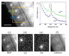
Fig. 1: Single molecular spectroscopy of mixed peapods (La@C82 and Ce@C82) at 30 kV[5]. (a) An ADF image with a rectangle showing where the spectrum image was taken. (b) Two EELS spectra recorded from two metal atoms. The atom indicated by the green arrow is assigned as La, and the other, indicated by the blue arrow, as Ce. (c) ADF image and (d, e, f) chemical maps for La, Ce, and carbon, respectively. Scale bar = 1 nm. |
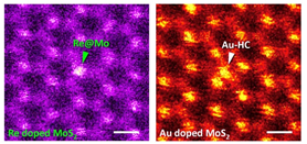
Fig. 2: Detection of single dopant atoms in single-layered MoS2[7]. (Left) An ADF image of Re-doped MoS2. The Re substitution at Mo site (Re@Mo) is pointed by a green arrow. (Right) An ADF images of Au-doped MoS2, where an Au adatom (indicated by a white arrow) located at the hollow-center (Au-HC). Scale bar = 0.3nm. |
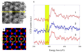
Fig. 3: Core-level spectroscopy of monovacancy in h-BN layer [8]. (a) ADF image shows a monovacancy in single-layer h-BN. Line spectrum was recorded along the yellow line. (b) Schematic presentation (red: nitrogen, blue: boron) of boron monovacancy. (c) Nitrogen K-edge fine structures extracted from the line-spectrum. Each of the three corresponds approximately to the probe positions marked in (b). A prominent pre-peak in the nitrogen K-edge can be found at 392 eV in the spectrum recorded at position 2, i.e., near the boron vacancy site. |
|