IT-10-P-5857 3D imaging of Si FinFETs by combined HAADF-STEM and EDS tomography
In last few decades electron tomography is intensively studied to recover the 3D shape of a wide range of nano-scale materials. High angle annular dark-field scanning transmission electron microscopy (HAADF-STEM) tomography attracts also increasing attention to study the morphology of semiconductor nano-devices with dimensions below 10 nm scale and a truly 3D morphology as instead of 2D projection images it provides 3D reconstruction with sensitivity along the beam direction. Recent advances of TEM systems with high brightness field emission gun (FEG) coupled with high count rate X-ray energy dispersive spectrometers (XEDS) opens the possibility to analyze the 3D volume both in imaging and chemical analysis modes.
Samples with dense Si fins (45 nm pitch) after Si etch, oxide fill and recess and thin epi-Si growth are explored. Pillar shaped specimens with various diameters are deposited on top of standard TEM grids and analyzed with Fischione conventional tomography holder. The work is done without gold markers, cf. fig 1, in a Titan cube 60-300 double aberration corrected system with SuperX EDS detector. Compared to lamella samples, the pillar configuration allows to increase the maximum tilt angle range from ~±65º to ±80º so that missing wedge effects are minimized. HAADF-STEM images are acquired in 1º steps and EDS maps each 5º. The STEM images are aligned and reconstructed by Inspect3D. Fig 2 presents the volume rendered 3D visualizations of the HAADF-STEM reconstruction and the orthoslices indicated in the volume. Si, SiO2 and FIB-damaged Si can be easily differentiated by the intensity. Moreover, Si and O X-ray maps are reconstructed separately with the same alignment. Fig 3 shows the superposition of both Si and O reconstructed volumes and the same corresponding slices as shown in fig 2. The orthoslices from the EDS reconstruction agree well to the HAADF-STEM reconstruction and also reveals the oxide grown on the Si fins. Compared to the 2D projection images, the orthoslices from the reconstruction indicate that the Si etch depth varies as indicated by blue arrows in fig 2c, 2d and fig 3c, 3d.
We show that the alignment can be done without marker tracking. The reconstructed volume based on HAADF images and EDS maps can bring useful fully interpretable information in composition and morphology unlike the 2D images that suffer from projection effects. Aberration corrected TEM improves the spatial resolution. Further analysis will involve using 360º tilt holder to fully eliminate the missing wedge artifacts and quantification of the elemental reconstructed volume, as well as application to next FinFET device processing steps involving gate and metallization steps.
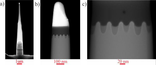
Fig. 1: Fig. 1 a) HAADF-STEM images of the pillar shaped specimen (diameter around Si fins area ≈ 240nm) on standard copper grid zoomed in b) and c) |
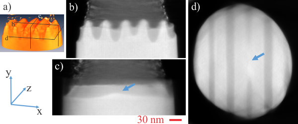
Fig. 2: Fig. 2 a) Volume rendered 3D visualization of HAADF-STEM reconstruction and its corresponding orthoslices in xy plane (b), yz plane (c) and xz plane (d) respectively |
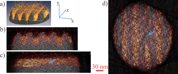
Fig. 3: Fig. 3 a) 3D chemical rendering of the Si fins and its corresponding orthoslices in xy plane (b), yz plane (c) and xz plane (d) respectively (gray : Si, yellow/red : SiO2) |
|