IT-4-P-5785 Time-Resolved Electron Beam Induced Current (TREBIC) Method for Spatiotemporal Analysis of GaN HFETs Structures.
GaN-based Heterostructure FETs are becoming preferable devices for high-speed and high-power applications in harsh environments. However, they suffer from the significantly deteriorated switching properties whose mechanisms are intensively investigated [1]. One of the possibilities to study spatiotemporal behavior of the device structures is to temporarily inject limited amount of charge using focused electron beam and to investigate the device’s time response. The lifetime in GaAs heterostructures was investigated by TREBIC in [2]. Combined time-resolved OBIC and TREBIC were used to map time response of InGaAsP/InP pin photodiode [3]. Dynamic behavior of HEMTs was investigated using backside infrared OBIC technique [4]. Stroboscopic TREBIC system was applied for analysis of dynamically biased power devices in [5].
In this contribution we report on the developed TREBIC system using sampling time-gated boxcar averaging techniques for spatiotemporal analysisof GaN based HFET structures. A field emission gun SEM equipped with beam-blanking system and multi-contact vacuum feedthrough has been used. Unpackaged HFETs soldered in a sample holder were connected to the feedthrough by 50 ohm coaxial cables. Induced current was detected by I/V converter (Figure 1). Alternatively, e-beam induced conductivity changes were detected, when a voltage on the resistor divider formed by resistor Rd and transistor channel Rch was preamplified by voltage amplifier. TREBIC signal in selected point or in selected area on sample was detected by digital oscilloscope with periodic signal used for beam-blanking. This technique offers excellent time resolution but it suffers from the huge amount of transferred data for each position of the e-beam [3]. Therefore, time-gated boxcar integration technique has been used to map the EBIC signal after selected delay Td from the rising edge of the e-beam (Figure 2). The gate width Tg determines the time resolution. Box car averaging of pulses was set as a compromise between the sensitivity and acquisition time. TREBIC signals measured from InAlN/GaN HFET device are shown in Figure 3, revealing slow response of the device to the charge injected in the G-D region of the transistor. From the series of TREBIC maps taken at various Td and Tg (e.g. in Figure 4) formation of a virtual gate in G-D region and inhomogeneous electric field build-up and recovery at the gate edge has been observed.
1. J.G.Tartarin et al., In: Proc. of the IWS 2013, IEEE, 2013
2. L.J. Balk et al., In: Proc. of the SEMAS, Part I, 447-456 (1975)
3. A. Šatka, J. Kováč, Microel. Eng. 24, 195-201 (1994)
4. D. Pogany et al., Microel. Reliab. 42, 1673-1677 (2002)
5. A. Pugatschow et al. In: Proc. of the 18th ISPSDIC, Naples, 2006, 4pp.
This work has been supported by the Slovak Research and Development Agency (contract No. APVV-0367-11) and by Slovak Grant Agency (project VEGA No. 1/0921/13).
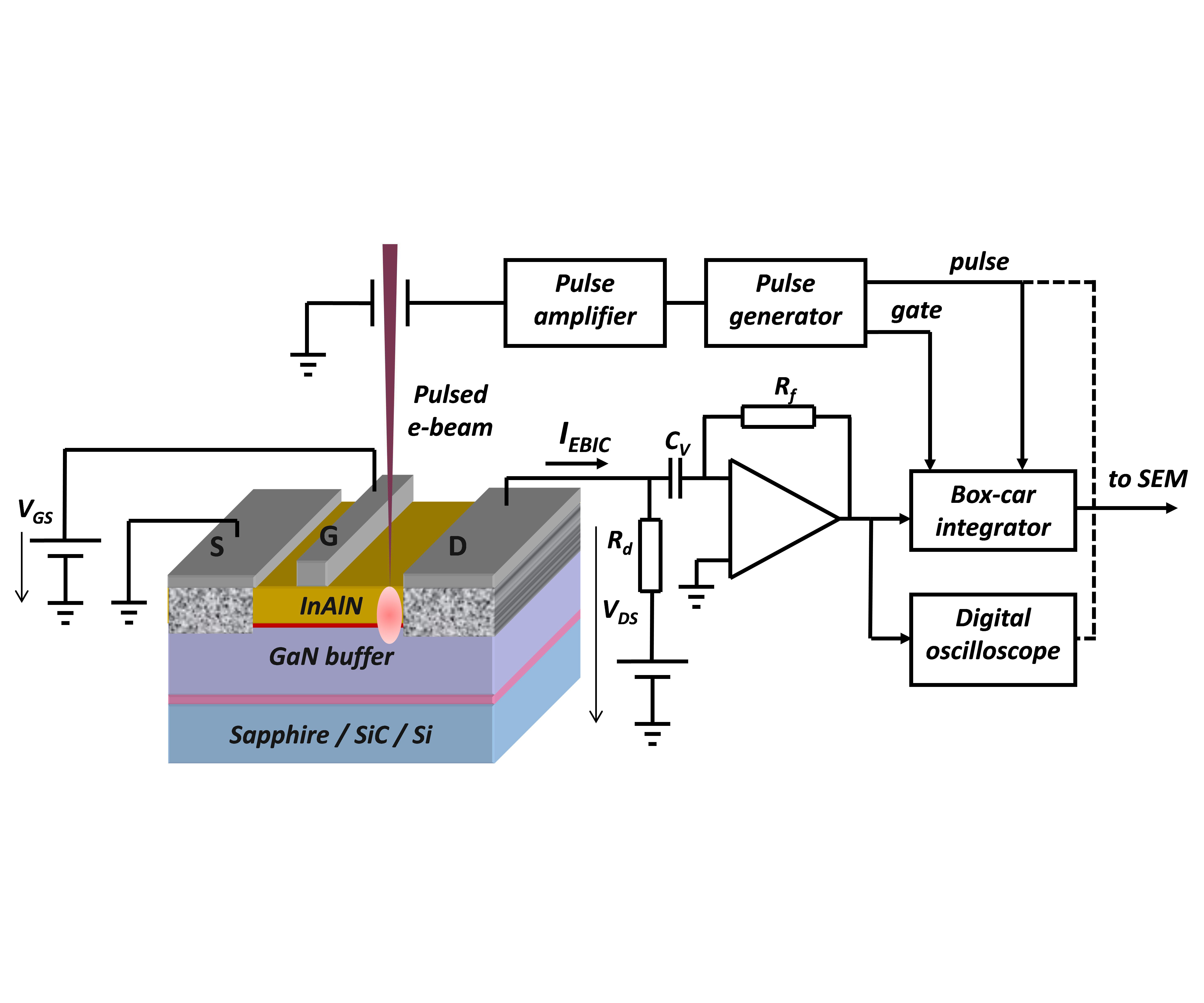
Fig. 1: Schematic drawing of the TREBIC experimental set-up using time-gated boxcar integration and oscilloscope techniques. |
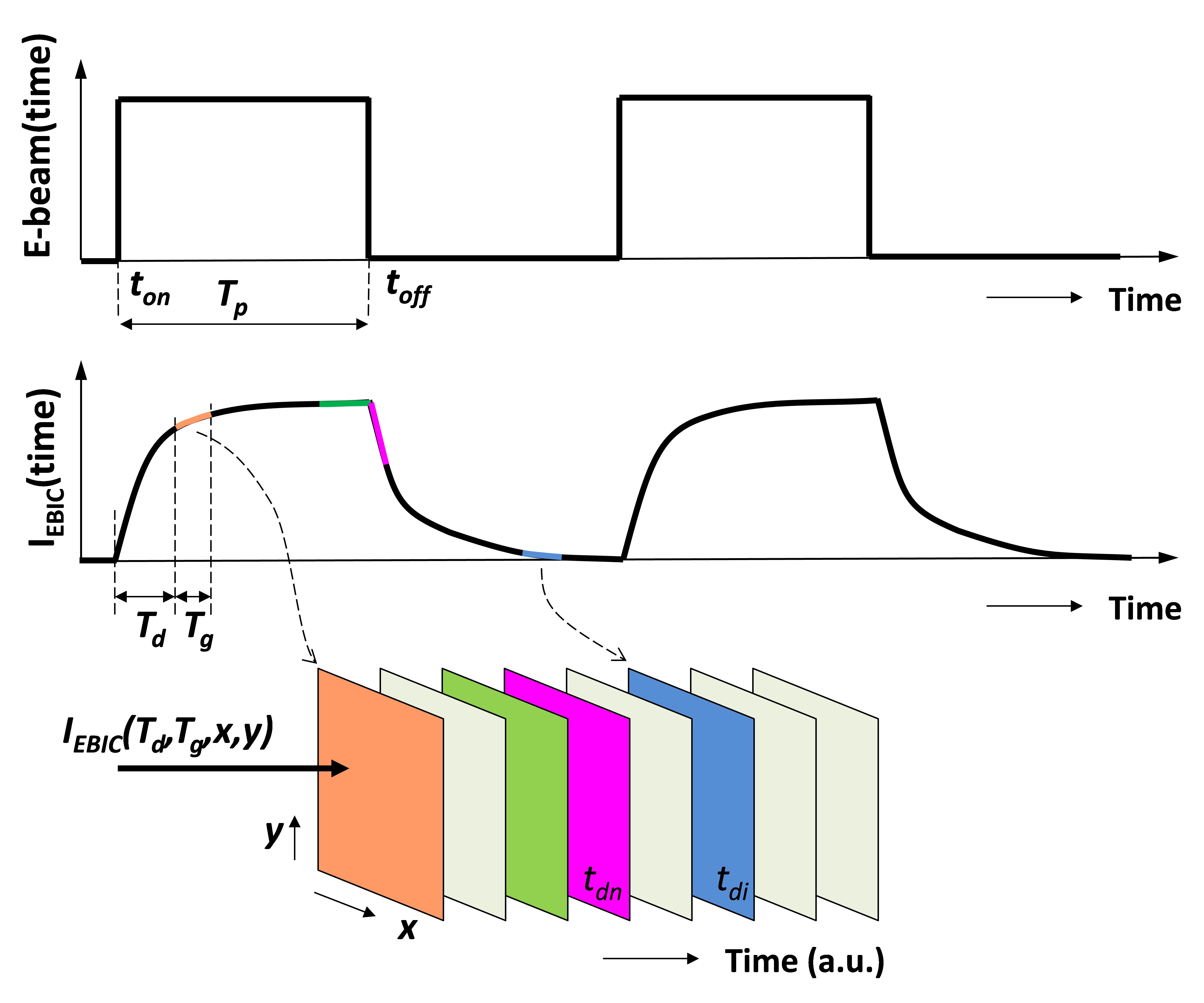
Fig. 2: Time dependence of induced current and formation of TREBIC maps. |
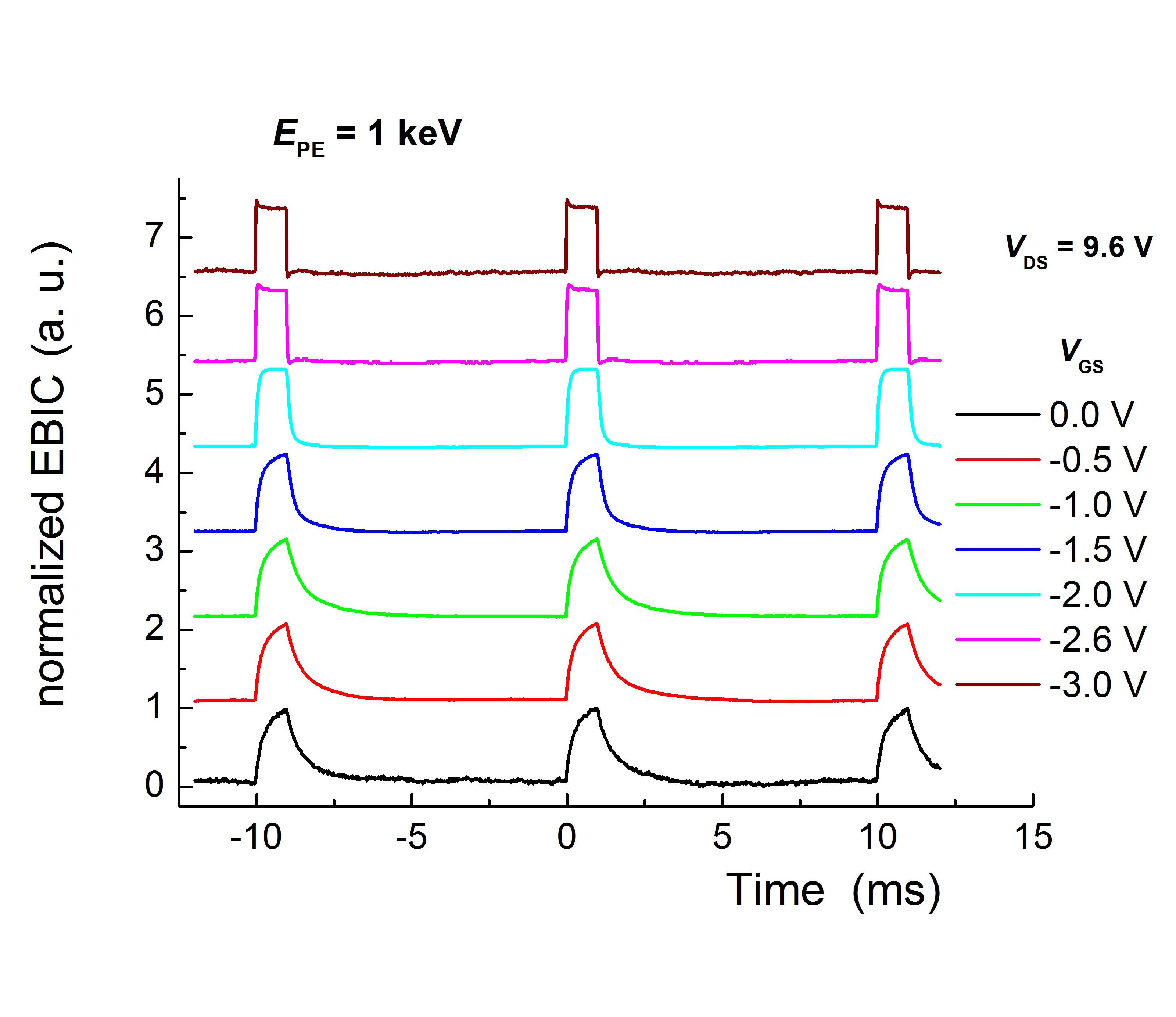
Fig. 3: Normalized TREBIC curves as a function of gate voltage VGS taken at VDS = 9.6V and e-beam energy Ebeam = 1 keV. |
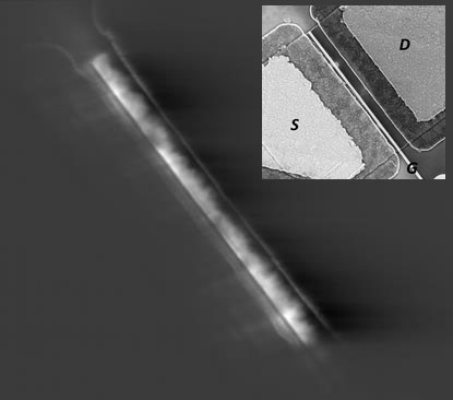
Fig. 4: TREBIC map taken from the top of HFET structure (see inset) immediately after the switching e-beam on (Td = 0 s) using gate width Tg = 3 ms. Pulse width Tp = 50 ms, VDS = 4 V, VGS = -4 V, Ebeam = 5 keV. |