IT-5-IN-5756 Advancing the spectroscopic frontiers of STEM
The field of electron energy-loss spectroscopy (EELS) has recently achieved a succession of impressive successes linked with the development of aberration correctors, enabling atomically-resolved spectroscopy, which are now spreading worldwide. In addition, a new generation of monochromators is emerging, providing improvements in energy resolution of at least one order of magnitude and giving unprecedented access to low energy-loss ranges. The possibilities in elemental analysis have become exceptional, especially as the progress in EELS has been accompanied by advances in energy-dispersive X-ray (EDX) analysis thanks to improvements in signal detection efficiency. Similarly, recent progress in the collection of visible-range photons emitted by a sample illuminated by a focused beam, has enabled novel cathodo-luminescence (CL) experiments in the scanning transmission electron microscope (STEM). In addition, new ways of exploiting fast electron beams, including combining them with beams of photons, have opened up the field of nano-optics, providing a high-spatial resolution alternative to more conventional optical techniques. Thus, STEM instruments are now extremely versatile, allowing for the simultaneous detection of an increasing variety of signals. Some of these new possibilities will be illustrated. For example, going beyond elemental mapping to measure fine structure (ELNES) variations at the scale of individual atomic columns or atoms will be described. Spectroscopic data acquired with EM or low-noise CCD cameras will be discussed in connection with the quantitative measurement of electron densities and the identification of charge ordering in oxide materials [1] or probing the chemical bonds of heteroatoms hosted in a carbon lattice [2]. Novel experiments combining EELS and CL, using a dedicated, home-made, high-efficiency nano-CL system will be presented, demonstrating how the usual macroscopic concepts such as extinction, absorption, and scattering cross-sections are no longer sufficient to describe optical phenomena at the nanoscale [3]. When used in combination with TEM structural investigations, nano-CL experiments have proved to be a unique way to explore the intimate link between a crystal structure (h-BN), its defects and its optical properties [4].
These experiments open stimulating perspectives for the development of further new spectroscopic techniques, combining photons and electrons in time-resolved applications for example, or entering the field of quantum optics.
[1] L. Bocher et al Phys.Rev. Lett. 111 (2013) 167202
[2] R. Arenal de la Concha et al, arXiv:1401.5007
[3] A. Losquin et al, submitted
[4] R. Bourrelier et al, arXiv:1401.1948
The work has received funding from the french CNRS-CEA METSA network and the European Programme ESTEEM2
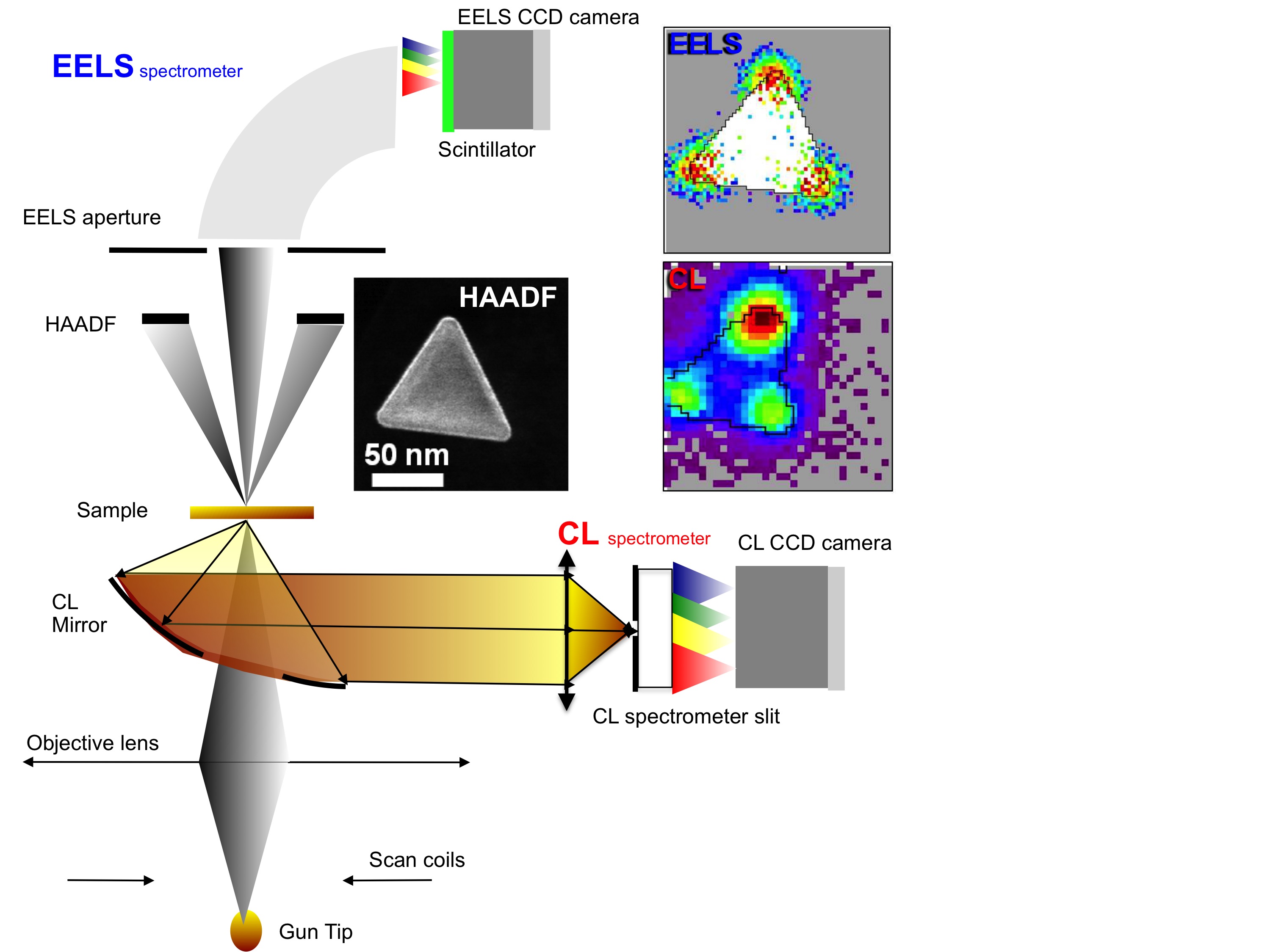
Fig. 1: Schematics of the Orsay STEM set-up dedicated to nano-optics experiments. The HAADF image of a gold nanoprism is shown in combination with the EELS and CL signal intensity maps (not acquired simultaneously in that specific case) revealing the spatial variation of the « tip » plasmon mode of the particle. |