IT-13-IN-5748 Development of cryogenic FIB-SEM based processes for organic and inorganic samples
Development of cryogenic FIB-SEM based processes Cryogenic EM is one of the best techniques we have to fix in place samples for EM that would otherwise be destroyed in the vacuum system [1]. Even though FIB-SEM has enabled a rapid, site specific and relatively easy way for TEM sample preparation it has not been easily adopted for cryogenically prepared samples. The impetus to develop a cryogenic sample preparation process with all the advantages of the room temperature one was high. However, the liftout and attach steps of the processes do not work in a cryogenic environment so either a more limited process had to be developed [2] or new equipment and new processes developed. Both have been achieved and we present here on the latter. This technique replicates the room temperature process but in cryo so that all of the developments surrounding FIB-SEM sample prep are available at cryogenic temperature. This not only requires a cold stage in the instrument but also sample transfer capability within and in-between each instrument involved. We describe this process, the equipment and modifications to it as well as applications. It was also discovered that certain inorganic material could benefit from cryogenic processing in FIB-SEM but for completely different reasons. Most FIB systems use gallium liquid metal as the ion sources (LMIS) and this species (Ga) can react chemically with certain compounds such as semiconductors to form undesirable side effects such as spheres and dots [3]. Milling under cryogenic conditions reduces these undesired reactions and in some cases this was the only way we could prepare the sample for TEM imaging (InN for example). We further investigated the effect of warm up after cryo milling for inorganic material and found that in most cases the undesirable side effects were minimized enough so that they did not interfere with our ability to image the sample. References [1] Adrian M., et al., “Cryo-Electron Microscopy of Viruses,” Nature 308, (01 March 1984), pp 32 - 36 [2] Rigort, A., et al., “Focused Ion Beam Micromachining of Eukaryotic Cells for Cryoelectron Tomography,” PNAS, (March 20, 2012), Vol. 109, No. 12, pp. 4449-4454. [3] Grossklaus, K. A., “Mechanisms of Nanodot Formation Under Focused Ion Beam Irradiation in Compound Semiconductors,” Journal of Applied Physics, Vol. 109 , Issue: 1, 2011, pp. 014319 - 014319-11.
The author acknowledges funding from the Center for Nanoscale Systems (CNS), a member of the National Nanotechnology Infrastructure Network (NNIN), which is supported by the NSF (under award no. ECS-0335765). CNS is part of Harvard University. I would also like to thank Dr. Ilan Shalish and Cheryl Hartfileld for their numerous contributions to this work.
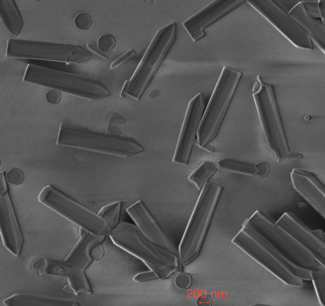
Fig. 1: InN nanoparticles grown in a forrest and felled for easier pickup. |
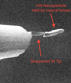
Fig. 2: A tungsten tip was sharpened to about 10 nm and used to pick up a single InN nanoarticle using only natural forces (Van der Waals). After pickup, the particle was placed on a TEM grid for milling in cryogenic conditions. |
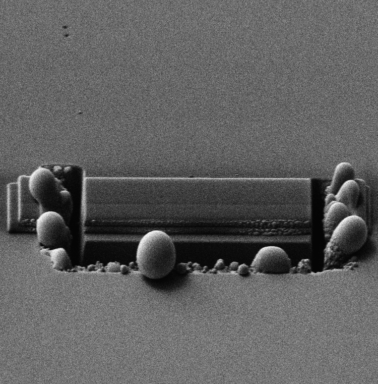
Fig. 3: GaN sample milled at room temperature using 1.5 nA FIB probe. The formation of dropplets is observed at room temperature and impedes clean milling of GaN. |
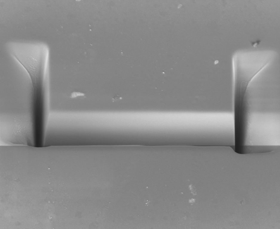
Fig. 4: GaN sample milled at -145 C using 1.5 nA FIB probe as in Fig. 3. The dropplets did not form as in the room temperature milling. |