IT-4-IN-5709 A review of SE and BSE imaging in SEM and Variable Pressure SEM
The SEM has evolved to a complex platform with multiple in-column and chamber-mounted SE and BSE detectors. With monochromated electron sources and biased stages the SEM can routinely provide sub-nanometre (0.4-7 nm) SE images and high voltages (15-30 kV), and in some cases low voltages (1 kV), on suitable samples. Live FFT analysis also now available on some instruments and it is particularly useful for high resolution operation. Another interesting and important development is the ability to collect images from the different detectors simultaneously, allowing consideration of the full range of sample information [figure 1], a consequence of higher resolution digital displays. The information content of the SE image is also much better understood, the in-column SED avoiding the well-documented but often forgotten “swamping” of the SE1 by SE2, SE3 and BSE through filtering and physical placement. Figure 1 also provides one example where surface contamination is most evident in the image from the in-column SED relative those from the BSED images and chamber-mounted SED image, even at high accelerating voltage (20 kV) and with C-coating. Stage tilt, reflecting angular selection, remains useful to enhance surface effects (such as relief in polished samples [figure 1b]). Electrostatic imaging of the chamber is a useful tool to illustrate the contribution of BSE generating SE3 on the pole piece and chamber walls in the vicinity of the E-T SED [figure 2b]. The angular sensitivity of BSE imaging has also been explored recently, particularly through the research of the late Heiner Jaksch in exploring the low angle BSE signals with ‘unconventionally’ short working distances. Two technologies have emerged, the use of in-column BSE detectors and selectable, segmented annular BSED. For example, the latter approach using a ‘tiled’, annularly-segmented single crystal Si diode detector [figure 2a] allows rapid switching through a range of collection angles, depending on the sample working distance. SE images in the variable pressure mode of SEM operation are strongly filtered by the positive ion cloud near and above the sample surface. The consequence is that such images lose the high resolution, near-surface component of the emitted SE. The collected signal is consequently dominated by higher energy SE and BSE and the deeper, delocalised ‘material’ contrast from the sample, even at the lower beam energies. It is currently difficult to envisage conditions in variable pressure mode where SE images will be directly comparable to those collected in high vacuum mode. The presence of a thin metal coating will assist. This filtering is not present where localized gas leakage is used for surface charge cancellation.
FEI, TESCAN, Hitachi HT, and JEOL have all generously provided time on instruments.
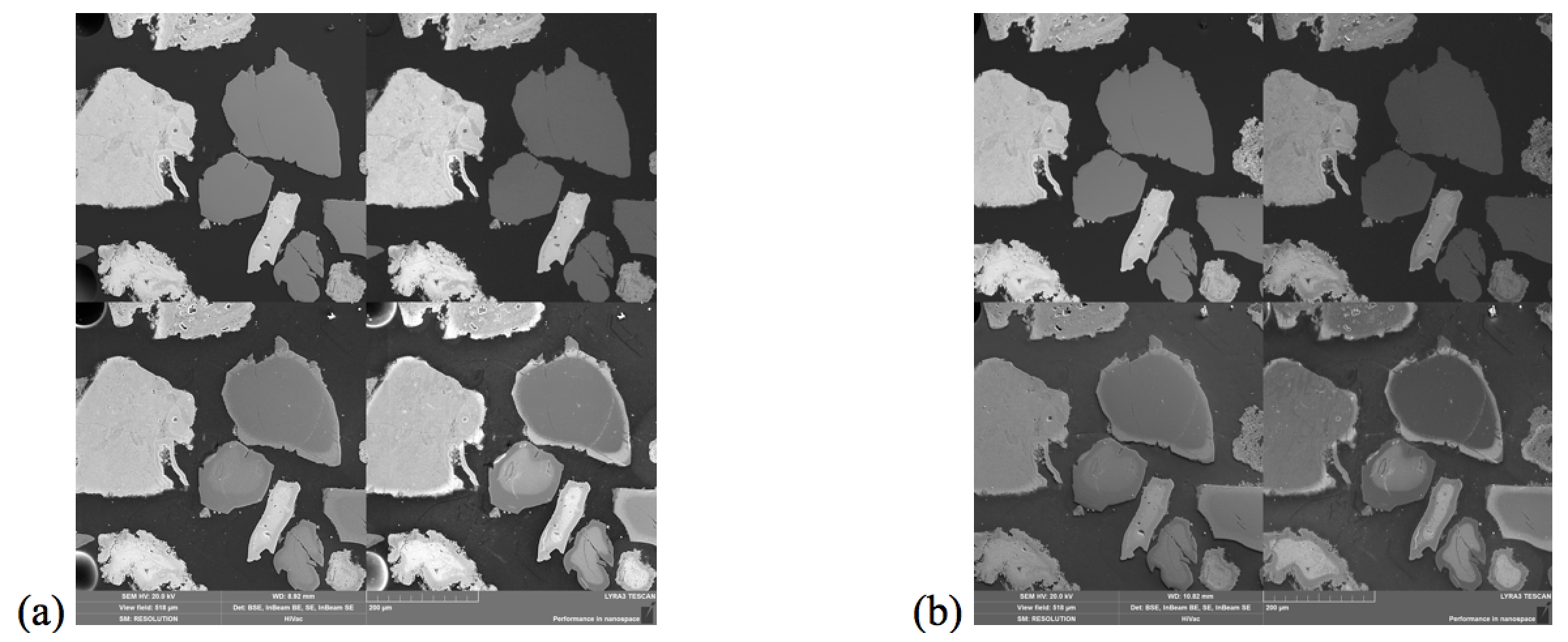
Fig. 1: Simultaneously collected images using (from top left and clockwise) chamber-mounted BSED, in-column BSED, in-column SED and chamber-mounted SED (E-T style) at zero (a) and 55 degree stage tilt (b), at 20 kV. Taken with the TESCAN Lyra3 FESEM. |
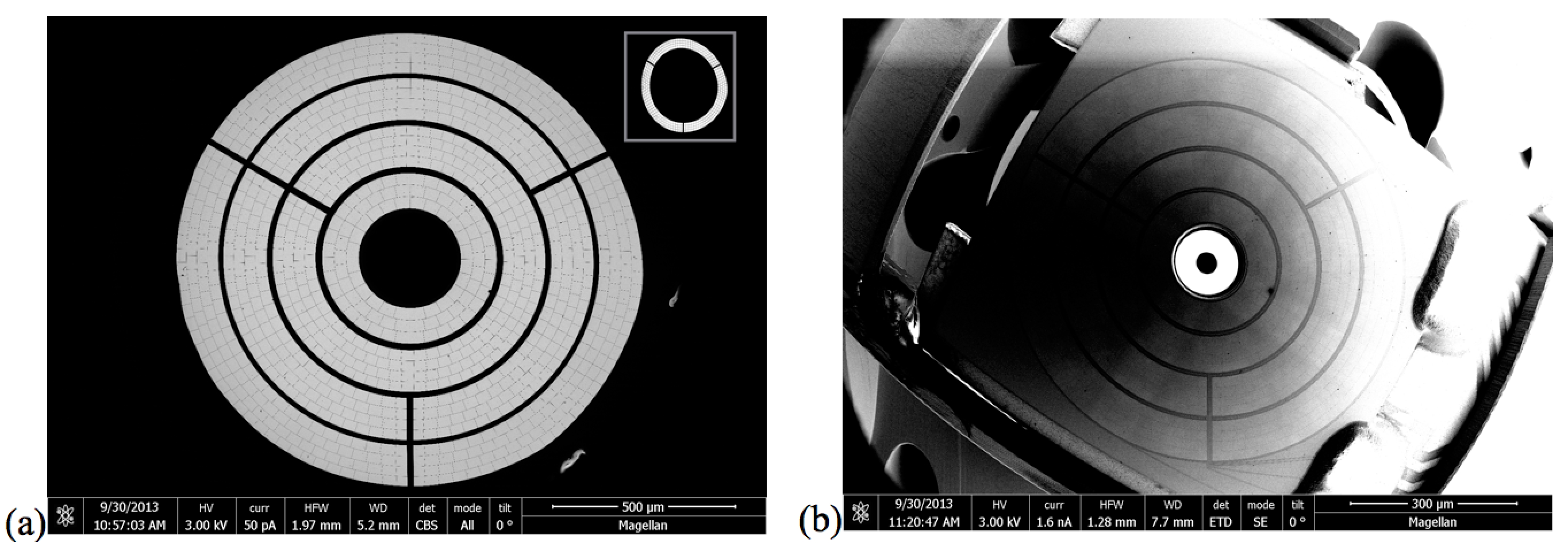
Fig. 2: Electrostatic mirror images using the BSED (a) and showing the ‘tiled nature and the 4 annular discrete segments (all active), the insert shows the outer segment active. The E-T SED image (b) shows channeling in the single crystal silicon BSED detector and highlighting due to SE3 from the immediate surrounds. Taken with the FEI Magellan XHR FESEM. |