IT-5-P-3513 Fabrication of High Energy Resolution Silicon Drift Detector for Energy Dispersive X-ray Spectrometer
Energy Dispersive X-ray Spectrometer (EDS) is the most common analytical equipment in SEM or TEM used for the elemental analysis or chemical composition of a sample. The most critical part in EDS system is the x-ray detector. The most common detectors are made of Si(Li) crystal. The major drawback of Si(Li) detector is that they require hours to cool down before use, and cannot be allowed to warm up during use. Besides, the increase of Si(Li) detection area will increase the capacitance that cause the increase of electronic noise. There is a trend towards a newer EDS detector over past decade, called the silicon drift detector (SDD). The key advantage of the SDD is the very lower anode capacitance compared with conventional silicon detectors of the same area. This unique feature reduces electronic noise and shortens processing shaping time to achieve higher energy resolution and counting rate. Due to the small anode in the SDD the leakage current is so low that the SDD can be operated with moderate cooling by Peltier cooler.
High resolution SDD have been designed, fabricated and tested.(Fig.2) The SDDs were fabricated on n-type<111> and a resistivity of more than 4kΩ.cm silicon substrates with a thickness of 400μm. The SDD consists of fully depleted silicon, in which an electric field with a strong component parallel to the surface drives electrons generated by the absorption of x-ray towards a small sized collecting anode. The electric field is generated by a number of increasingly reverse biased cathodes on one side surface of the device. The radiation entrance window on the opposite side is made by a non-structured shallow implanted junction giving a homogeneous sensitivity over the whole detection area.
SDD comprise homogeneous radiation entrance window and the anode guard ring for improving the energy resolution of detector.(Fig.1) First, if the p-n junction is located at deep depth, the thickness of dead layer will to thick. Therefore the homogeneous window is important to control the loss of entrance X-ray. Detailed studies showed that a 1100-1200 Å thick layer of aluminum sufficiently attenuates visible light so that it has a negligible impact on the SDD leakage current. Second, in the detector all electrons generated at the Si/SiO2 interface are collected on the anode guard ring rather than contributing to the detector leakage current.
SDD were characterized to extract critical I-V performance parameter like total leakage current at anode. The value of leakage current of ring_2 is 248 nA without anode guard ring, and reduces to 4 nA with anode guard ring.(Fig.3) And will test the response for detector exposed to the X-ray source in the future. The goal of the testing have shown a FWHM at MnKα line of a radioactive 55Fe source of 170 eV at -20℃.
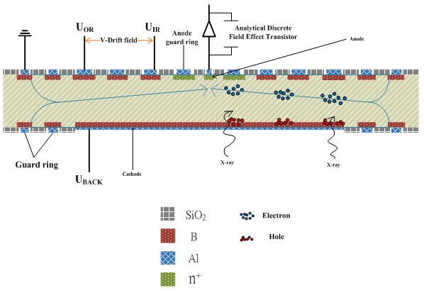
Fig. 1: Cross section and operation scheme of a SDD detector with anode guard rings and non-structured homogeneous x-ray entrance window. |
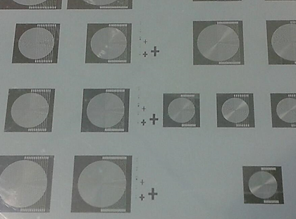
Fig. 2: Photo image of a fabricated silicon drift detectors. |
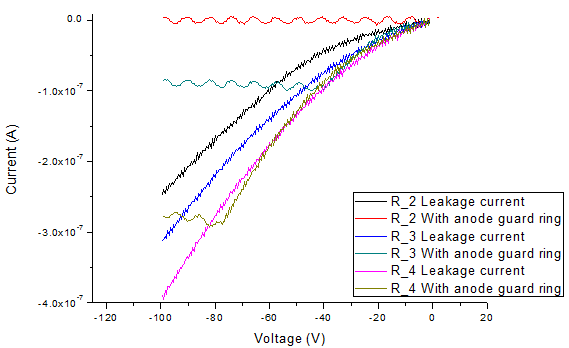
Fig. 3: Leakage current of SDD with testing anode guard ring. |
|