IT-4-P-3491 Application of Ultra Low Voltage Secondary and Backscatter Imaging in FE-SEM for Imaging of Nanomaterials
Significant advances in electron optics and detectors in field emission scanning electron microscope (FE-SEM) in the last decade have allowed the researchers to observe a variety of materials and biological specimens with ultra-high resolution and exceptional surface detail. In particular, low voltage imaging has been successfully employed as a key technique for charge control and reduction. Enhancements in electron column optics towards smaller chromatic and spherical aberration coefficients, with improved ability to deal with charging specimens via precise control of the landing energy of impact electrons and electron signal detection through in-column signal filtering or signal collection angle control have opened new avenues for specimen observation [1]. These new design improvements have significantly advanced the ability to image insulating specimens with previously unattainable nanometer scale resolution [2] at landing voltages as low as 10V (Fig. 1). In this paper we will discuss common approaches and challenges associated with ultra-low voltage imaging. The instrument employed for these studies is JSM-7800F ultra-high resolution FE-SEM that features a hybrid lens design and the ability to bias the specimen stage thus decelerating the primary beam (Gentle Beam). When beam deceleration is employed the accelerating voltage which along with lens aberrations determines the minimum probe size and thus the resolution limit is retarded by a negatively charged bias to a lower landing energy. The landing voltage can be varied to achieve the necessary charge balance as well as high resolution performance at ultra-low voltages. Beam deceleration also serves as a form of aberration correction [3]. The use of Gentle Beam function preserves all the advantages of high kV imaging (gun brightness, small probe size) with added advantages of reduced charging, reduced specimen contamination and improved surface detail. Moreover, through-the-lens detection system features an ability to precisely filter the detected signal, providing the user with an additional degree of control during the imaging. We will demonstrate our experiences with imaging a variety of specimens, such as zeolites, biological nanostructures, oxides, nano-structured metals and more. The advantages of low kV imaging for such techniques as cathodoluminescense imaging and voltage contrast will be highlighted. Additional methods for charge balance, such as reduced probe current and adjustment of scan speed will also be discussed. References: [1] D.C. Bell and N. Erdman. Low Voltage Electron Microscopy: Principles and Applications (2012) [2] S. Asahina et al., Microscopy and Analysis, (2012) p.S12. [3] L. Frank and I. Müllerová, Ultramicroscopy, 106 (2005) p. 28
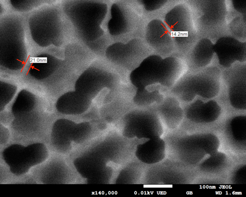
Fig. 1: Anopore membrane filter imaged uncoated at 10V. Pore walls (14 and 21 nm) are clearly resolved. |