IT-5-O-3427 Elastic scattering of atomic-size electron probes carrying orbital angular momentum in aberration-corrected scanning transmission electron microscopy
The pioneering work by Uchida and Tonomura in 2010 [1] showed that electron beams carrying orbital angular momentum (OAM) can be produced in a transmission electron microscope. Since then, there has been a large interest in the microscopy community to produce atomic-size electron probes carrying OAM [2,3]. The interest arises because using those probes, in principle, one could study magnetic dichroism at the atomic scale through electron energy-loss spectroscopy (EELS) in aberration-corrected scanning transmission electron microscopy (STEM) [2].
In this work, we will present calculations that show how an atomic-size electron probe carrying OAM (vortex probe) channels through the sample and how its OAM character is affected by channeling. We will discuss the reasons why STEM images using vortex probes seem to show lower intensity contrast than images obtained with conventional aberration-corrected probes (as the example illustrated in Figure1). The STEM images simulations were obtained with a multislice algorithm scheme, using a recently developed code in Python (pySTEM) at Oak Ridge National Laboratory. The code calculates electron probes (up to C7 aberrations) with OAM implemented following the electron optics setup outlined in Refs. 4 and 5.
References:
[1] M. Uchida and A. Tonomura, Nature 464, 737 (2010).
[2] J. Verbeeck et al., Nature 467, 301 (2010).
[3] B. McMorran et al., Science 331, 192 (2011).
[4] J.C. Idrobo & S.J. Pennycook, J. of Electron Micros. 60, 295 (2011).
[5] O.L. Krivanek, et al., Micros. Microanal. in press (2014).
This research was supported by ORNL’s Center for Nanophase Materials Sciences (CNMS), which is sponsored by the Scientific User Facilities Division, Office of Basic Energy Sciences, U.S. Department of Energy (JCI).
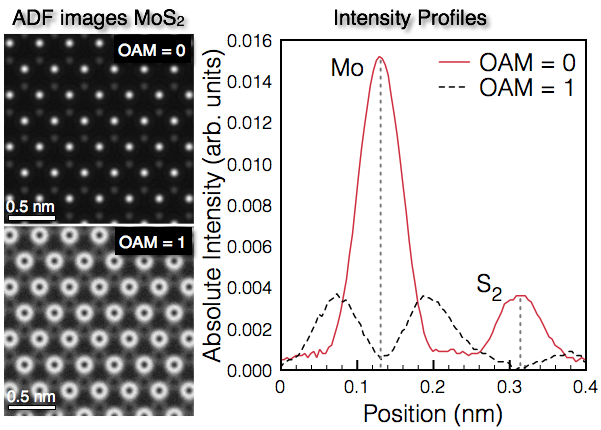
Fig. 1: (Left) Simulated ADF images of monolayer MoS2 with an electron probe with and without orbital angular momentum (OAM). Simulations done at 100 kV, a converge semi-angle of 30 mrad, and ADF collection semi-angles of 81-200 mrad. (Rigth) Intensity profile along the centers of a Mo atom and a S2 atomic column. Intensity profile width of 0.16 nm. |