IT-13-P-3393 USING THE FOCUSED ION BEAM MICROSCOPE TO DEVELOP DIFFRACTION GRATINGS FOR QUANTUM WELL INFRARED PHOTODETECTORS
Quantum well infrared photo detectors (QWIP) has several advantages when compared to other kinds of IR detectors, but it requires an optical coupling in order to work due to the quantum selection rule. These detector must has a Electrical Component of radiation (TE) parallel with structures grown direction. Diffraction gratings are one of the several types of optical coupling suitable to be implemented on these detectors. In this work we opt by diffractions gratings because the best optical coupling if compared with other techniques (1).
Due to the wavelengths of interest in this work (4,1um) and the refraction index the detector's material (n = 3.2) the features of the such gratings are almost sub-micrometric (2). The processes of optical lithography currently available in Brazil do not allow the fabrication of these diffraction gratings, essential to the functioning of these IR detectors, with the theoretical dimensions recommended, especially for near and mid infrared (3). The Focused Ion Beam microscope (FIB) allows the fabrication of these structures at resolutions more than enough (4) (5) (6).
The study and fabrication of these gratings are the objects of this work. FIB was used in the manufacture of gratings with several dimensions, from the theoretical dimensions until the optical lithographic dimensions (Figure 1) on QWIP mesa devices fabricated by usual optical lithography, enabling the investigation of the possible loss of electrical response of the QWIP´s detectors if they were textured with the available optical lithographic processes currently in Brazil.
To characterize the dimensions of arrays was used Atomic Force Microscopy (Figure 2). After fabrication diffraction gratings was deposited In each individual mesas a thin Gold film (180nm) to make the electric contacts by gold wire bonding (Figure 2a,b ).
This chip was assembly in header where the electric response the individual mesas will be measured and compared (Figure 3). The features of dimensions these gratings and their effect on the electric response of the devices will be presented.
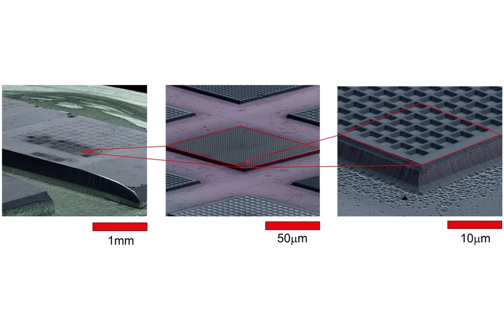
Fig. 1: Figure 1 – SEM image of the photodetector mesas after fabrication of diffraction gratings |
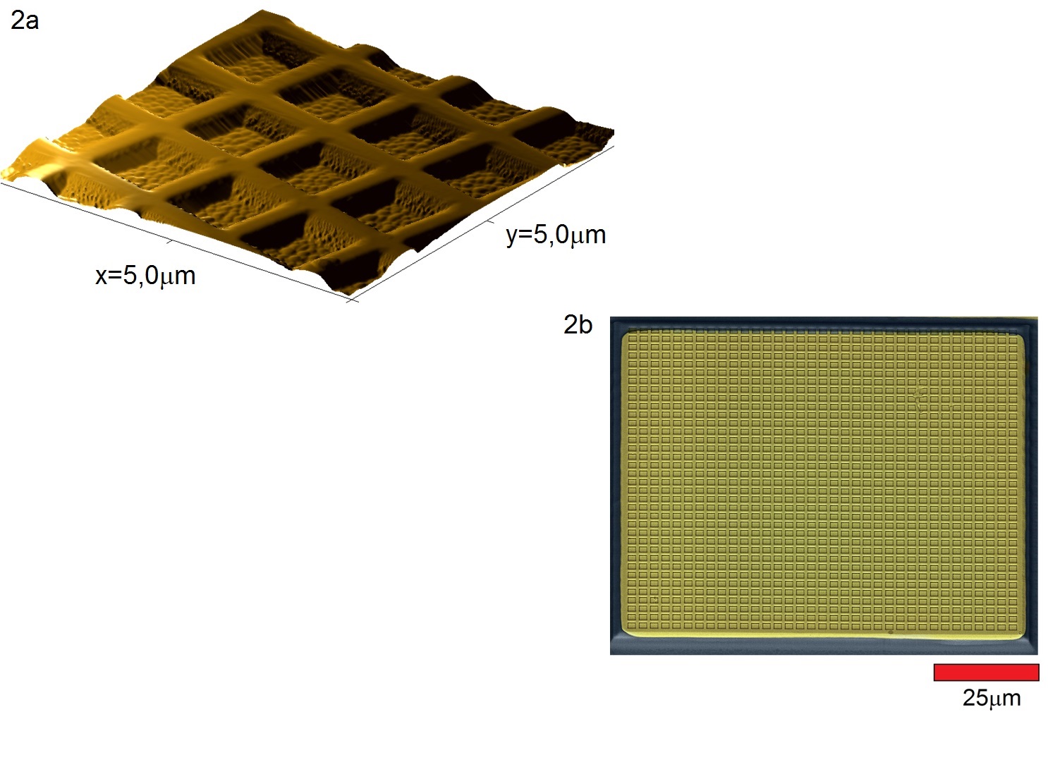
Fig. 2: Figure 2a – AFM Image of a diffraction grating. Figure 2b – SEM image of one already textured mesa with the deposited ohmic contact |
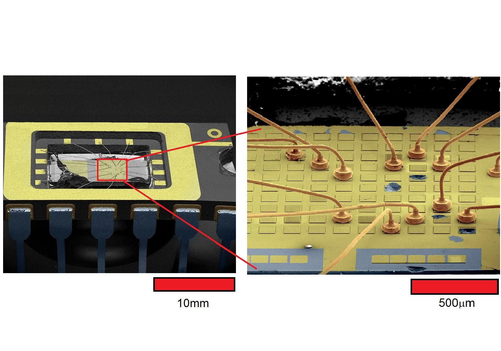
Fig. 3: Figure 3 – SEM image of the chip assembled on the header and SEM image of the wire bonded mesas on the header |
|