IT-13-P-3258 FIB as Fabrication Tool for Advanced Analytical Infrared Sensing Schemes
Within the last decade, focused ion beam (FIB) technology emerged as a universal tool, for maskless prototyping via highly localized milling and deposition processes. FIB prototyping is particularly interesting for analytical devices such as novel optical sensing structures for the mid infrared (MIR) regime and functionalized scanning probes [1].
The MIR (3-12µm) spectral range is particularly interesting for biosensing applications, since it provides inherent molecular selectivity. MIR photons interact with most organic and inorganic molecules by excitation of vibrational und rotational modes [2-5].
Quantum cascade lasers and semiconductor thin-film waveguides facilitate highly sensitive optical biosensors for the MIR regime. Among those biosensors, the Mach-Zehnder interferometer (MZI) is one of the most promising sensor as it can be fully integrated in a lab-on-a-chip microsystem and provides high sensitivity.
The developed MIR-MZIs are chip-integrated solid-state devices based on GaAs/Al0.2Ga0.8As technology wave guide fabricated via conventional optical lithography and reactive ion etching (RIE). Since optical lithography is limited to a resolution of about 2 µm, the microfabricated devices were further structured via FIB milling for minimizing scattering losses at the Y-junction, and to increase the optical throughput.The radius of the Y-junction edges was reduced from about 2 µm to less than 100nm, thereby leading to a throughput enhancement of more than 30% of incident light in comparison to structures without FIB milling (Fig. 1)[6].
Grating couplers are another way for minimizing coupling losses, especially for wave guide with micro- to nanoscale dimensions. FIB milling of grating couplers is a reproducable and reliable strategy for launching radiation into a wave guide structure and improving the overall performance of the optical device [7].
References:
[1] C. Charlton, B. Temelkuran, G. Dellemann, B. Mizaikoff, Appl. Phys. Lett., 86, 194102 (2005).
[2] C. Charlton, M. Giovannini, J. Faist, B. Mizaikoff, Anal. Chem., 78, 4224-4227 (2006).
[3] C. Young, S.-S. Kim, Y. Luzinova, M. Weida, D. Arnone, E. Takeuchi, T. Day, B. Mizaikoff, Sens. &Act. B, 140(1), 24-28 (2009).
[4] X. Wang, S.-S. Kim, R. Roßbach, M. Jetter, P. Michler, B. Mizaikoff, Analyst, 137, 2322-2327 (2012).
[5] A.Eifert, W. Smirnov, S. Frittmann, C.E. Nebel, B. Mizaikoff, C. Kranz, Electrochem. Commun. 25 (2012) 30-34
[6] M. Sieger, F. Balluff, X. Wang, S.-S. Kim, L. Leidner, G. Gauglitz, B. Mizaikoff, Anal. Chem., 85, 3050-3052 (2013).
[7] T. Schädle, A. Eifert, C. Kranz, Y. Raichlin, A. Katzir, B. Mizaikoff Applied Spectroscopy, 67, 1057-1063 (2013).
[8] X. Wang, M. Sieger, B. Mizaikoff, Proc. SPIE 8631, Quantum Sensing and Nanophotonic Devices X, 86312M (2013)
The authors gratefully acknowledge support for parts of this work by the Kompetenznetz Funktionelle Nanostrukturen Baden Wuerttemberg, Germany. Finally, the Focused Ion Beam Center UUlm is thanked for providing prototyping and characterization facilities during the present studies.
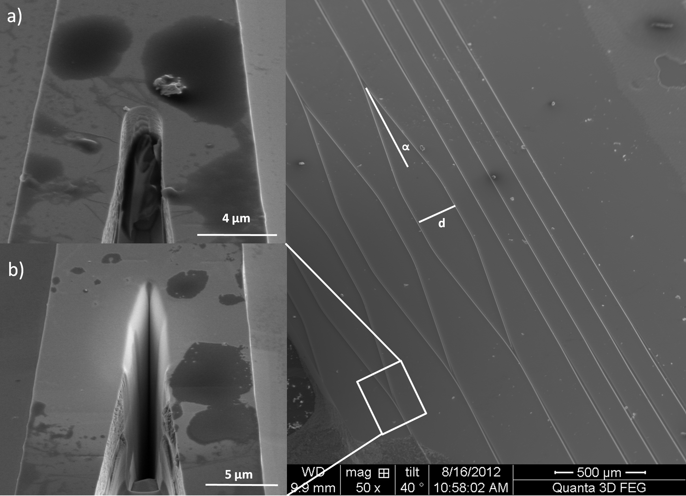
Fig. 1: Figure 1. Scanning electron microscopy (SEM) images of GaAs/AlGaAs MIR-MZI waveguides with different opening angles α and a constant distance between the arms d: (a) top view of a Y-junction before, and (b) after FIB milling process [8]. |