IT-4-P-3232 PERFORMANCE OF YAG:Ce SCINTILLATORS FOR LOW-ENERGY ELECTRON DETECTORS IN S(T)EM
Cerium activated single crystals of yttrium aluminium garnet (YAG:Ce) Y3-xCexAl5O12 are widely used as scintillators in electron detectors for S(T)EM [1]. Nowadays, it is sometimes necessary to detect low-energy electrons without post-acceleration. In such cases, extremely sensitive detectors are required that are able to detect even electrons with energies of only hundreds of eV while avoiding charging of the scintillator surface. However, commonly used scintillators strongly lose their light yield with the decrease of the incident electron energy [2]. Moreover, a thinner conductive layer on the scintillator surface has to be used to allow low-energy electrons to pass through. Possible charging of the surface negatively affects its cathodoluminescence (CL) light yield. The low-energy electron excitation takes place closer to the scintillator surface where damage can be expected owing to its preparation, which also reduces the CL light yield. The aim was to study the influence of the scintillator and its conductive layer on the low-energy electron detection efficiency.
In general, the following demands are made of the conductive layer: it should have the highest possible optical reflectivity, conductivity and electron transparency. These demands are mostly met for metals with a low atomic number. However, if the layer is very thin, it can form “islands”, i.e. a non-continuous layer of drastically decreased conductivity. We decided to apply scandium as a possible option. The YAG:Ce single crystals were studied using both Monte Carlo simulation and CL measurement. The MC method (Fig. 1) used Mott cross-sections and the Bethe slowing-down approximation. Using the CL apparatus (Fig. 2) [3], incident electron energy can be changed from 0.8 to 10 keV. The detection dynamic range spans 5 orders of magnitude. The experimental results are shown in Fig. 3. The significant decrease of efficiency at lower energies may be caused by the layer which doesn’t allow more electrons to pass through, by the YAG:Ce single crystal that has a lower light yield near the surface, and finally, if the layer isn’t conductive enough, it can be charged and retard incident electrons. Even so, we have found that the YAG:Ce scintillator with a 3 nm scandium layer is applicable for the detection of electrons having an energy as low as 800 eV.
References
[1] P. Schauer, Nucl. Instrum. Methods Phys. Res. B 21 (2011) 2572–2577.
[2] G. F. J. Garlick, Brit. J. Appl. Phys. 13 (1962) 541–547.
[3] J. Bok, P. Schauer, Rev. Sci. Instrum. 82 (2011) 113109.
Thanks are due to CRYTUR, Ltd., for the supply of scintillators, to J. Sobota for the preparation of scandium layers, to the Technology Agency of the Czech Republic (TE01020118), to the European Commission and to the Ministry of Education, Youth and Sports of the Czech Republic (CZ.1.07/2.3.00/20.0103).
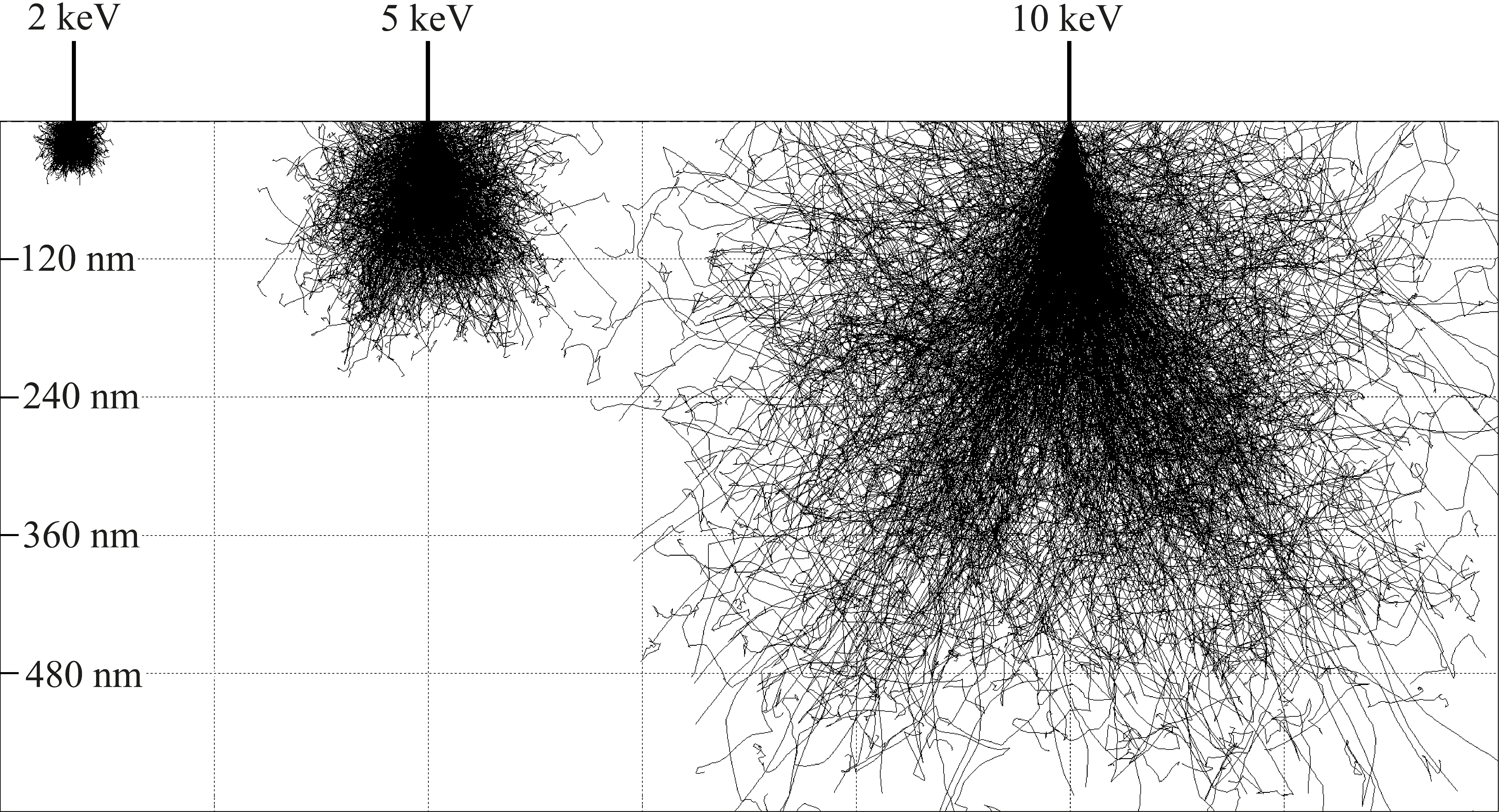
Fig. 1: Interaction volumes in the YAG:Ce single crystal simulated by the Monte Carlo method. Simulated without any conductive surface layer. |
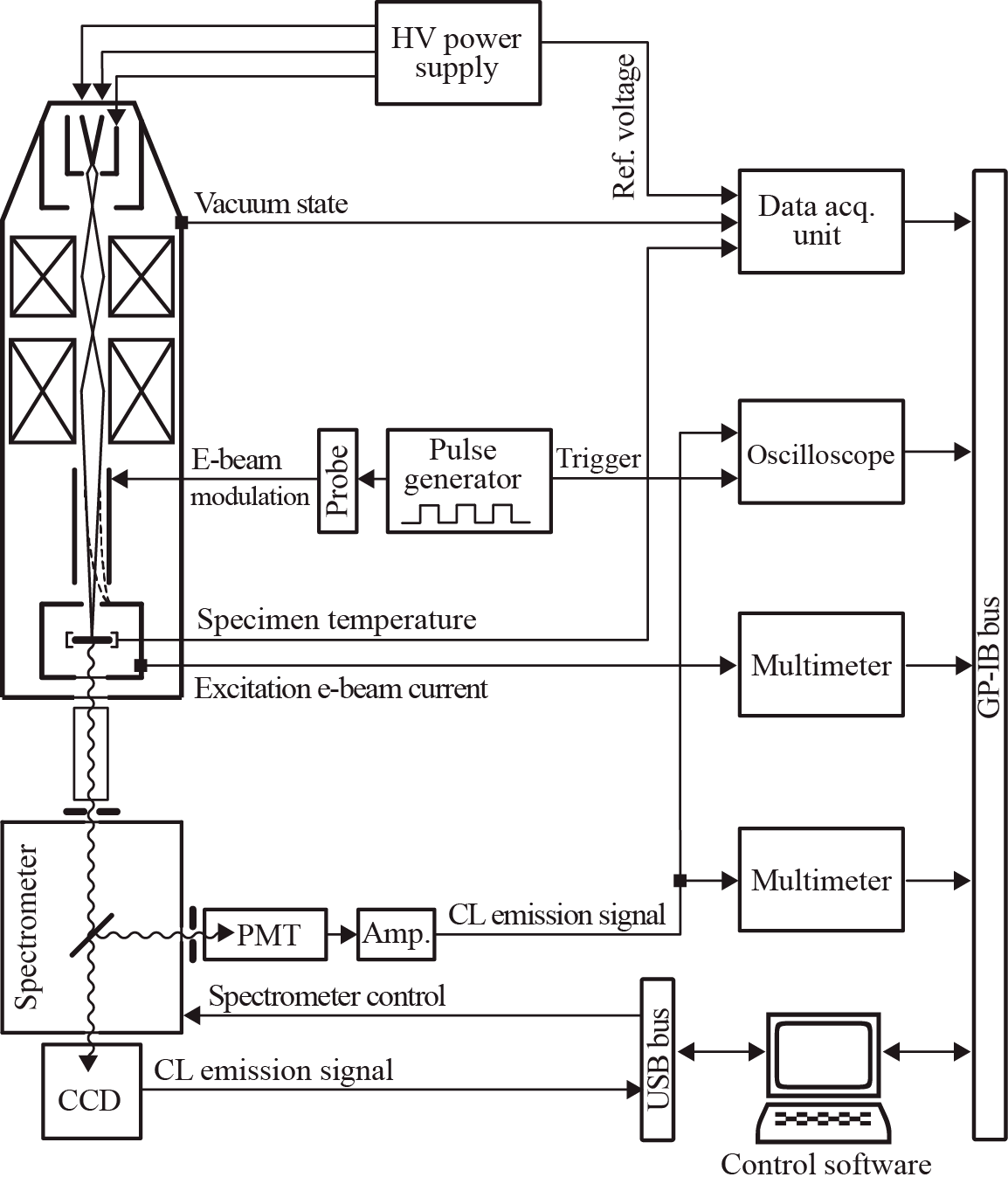
Fig. 2: Experimental equipment used for cathodoluminescence (CL) property measurements. |
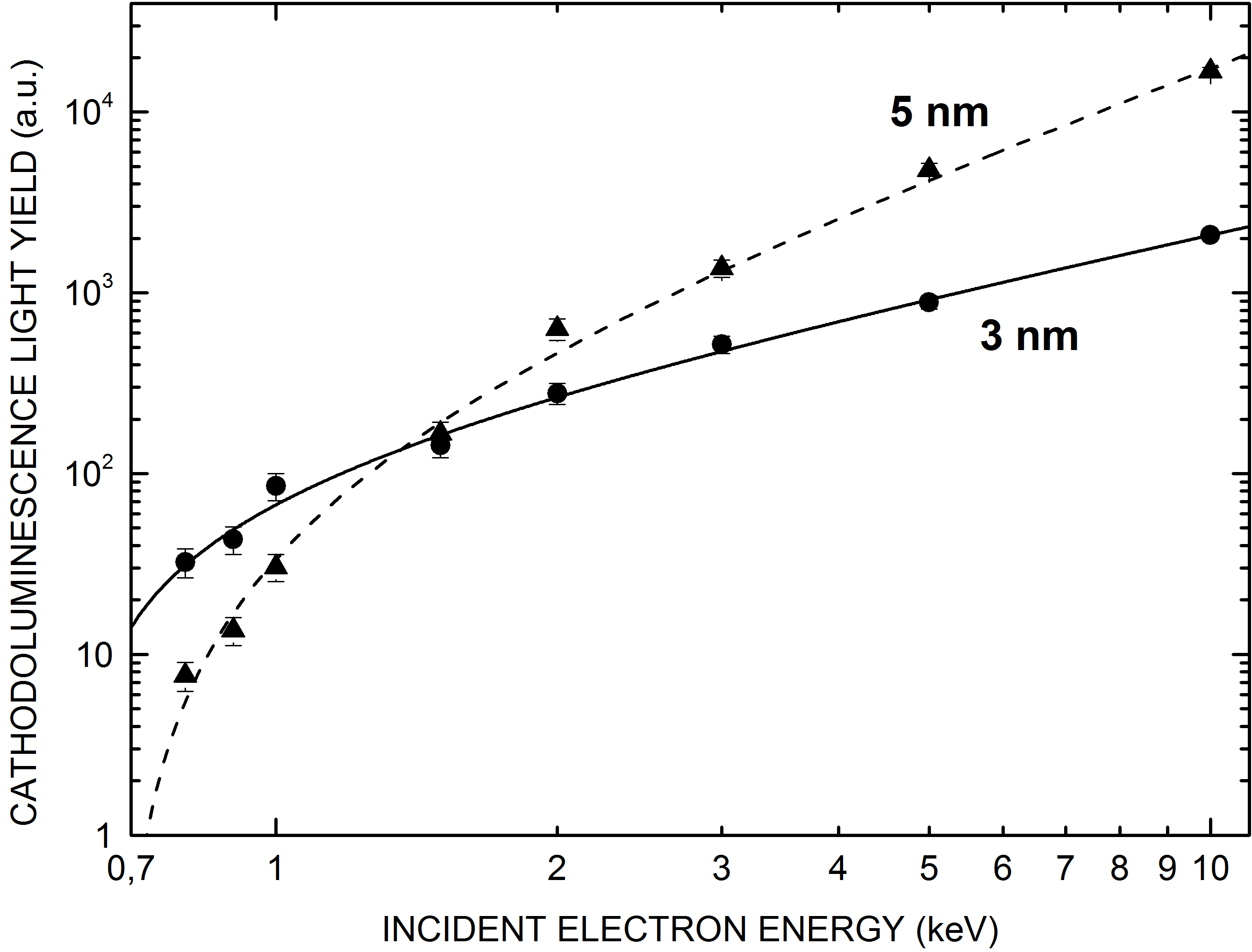
Fig. 3: The cathodoluminescence light yield of the YAG:Ce single crystal scintillator coated with a scandium layer of a thickness of 3 and 5 nm, respectively, as a function of the incident electron energy. |
|