IT-14-IN-3211 Theory of Near-Field SEM: lateral resolution, scaling properties and compact equations
A new form of lenseless microscopy called near-field emission scanning electron microscopy (NFESEM) has been devised at ETHZ. In this form of microscopy the emitting tip is placed at a distance d of a few nm away from the sample (anode) with no focusing device in between. Besides the obvious advantages of price, NFESEM can perform DOS analysis (as STM) but also chemical identification by looking at the backscattered (or secondary reemitted) electrons.
The vertical resolution of this form of microscopy is as good as that of other forms of microscopy but the lateral resolution is about 3 nm at d=25nm and can be improved to 1 nm at smaller d. The latter constitutes a surprisingly good result considering the absence of a lens but it is not understood with conventional field emission theory. In this paper we present ab initio 3-dimensional WKB calculations applied to an ellipsoidal emitting tip that can explain the good lateral resolution capabilities of NFESEM. In particular, we show that the electron trajectories converge faster to the vertical direction compared to spherical emitting tips. This process begins in the classically forbidden (or tunneling) region where, contrary to accepted wisdom, electron paths may bend (see figure 1). As an end result of our calculations the beam spot size as a function of tip-anode distance d is obtained (figure 2)
The current-voltage (I-V) characteristics of this device are obviously d dependent. However for d>R=radius of curvature of the emitter, these characteristics show a remarkable property: all I-V curves fall onto each other when the applied voltage V is scaled (multiplied) by a single scaling function S(d), see figure 3. The explanation of this is rudimentary for image rounded linear potentials but for non-linear tunneling potentials U as those of nanoscopic emitters it demands a thorough investigation of the non-linear terms of U which we give.
Finally, in the course of our investigations, we have managed to produce- by strict mathematical proof- a generalized Fowler-Nordheim equation which is valid for any shape of surface. The accuracy of our equation – estimated by comparison to ab initio calculations- depends on R. For R>10nm it gives excellent results, for 5nm<R<10nm it gives satisfactory results and for R<5nm it does not work so well but still it gives much better results than the traditional FN equation, see figure 4.
This work would not have been possible without the substantial contributions of my former postdoc Dr Gerry Kokkorakis and my present PhD student Andreas Kyritsakis
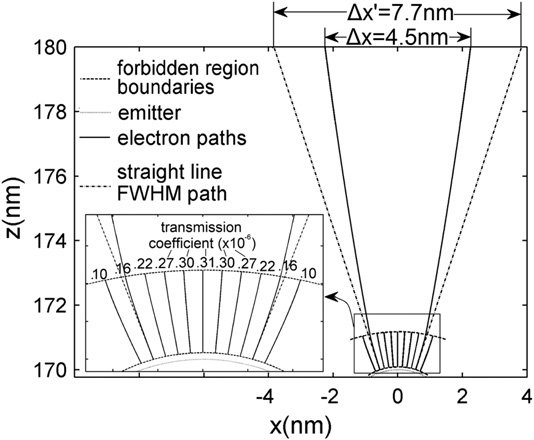
Fig. 1: Comparison of beam-spot diameters by usuing straight line paths and curved paths calculated by a 3-Dimensional WKB method |
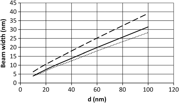
Fig. 2: Lateral resolution of an ellipsoidal NFESEM emitter as a function of tip-anode distance d. The various curves are for different combinations of the large and small radii of the elliptical tip. |
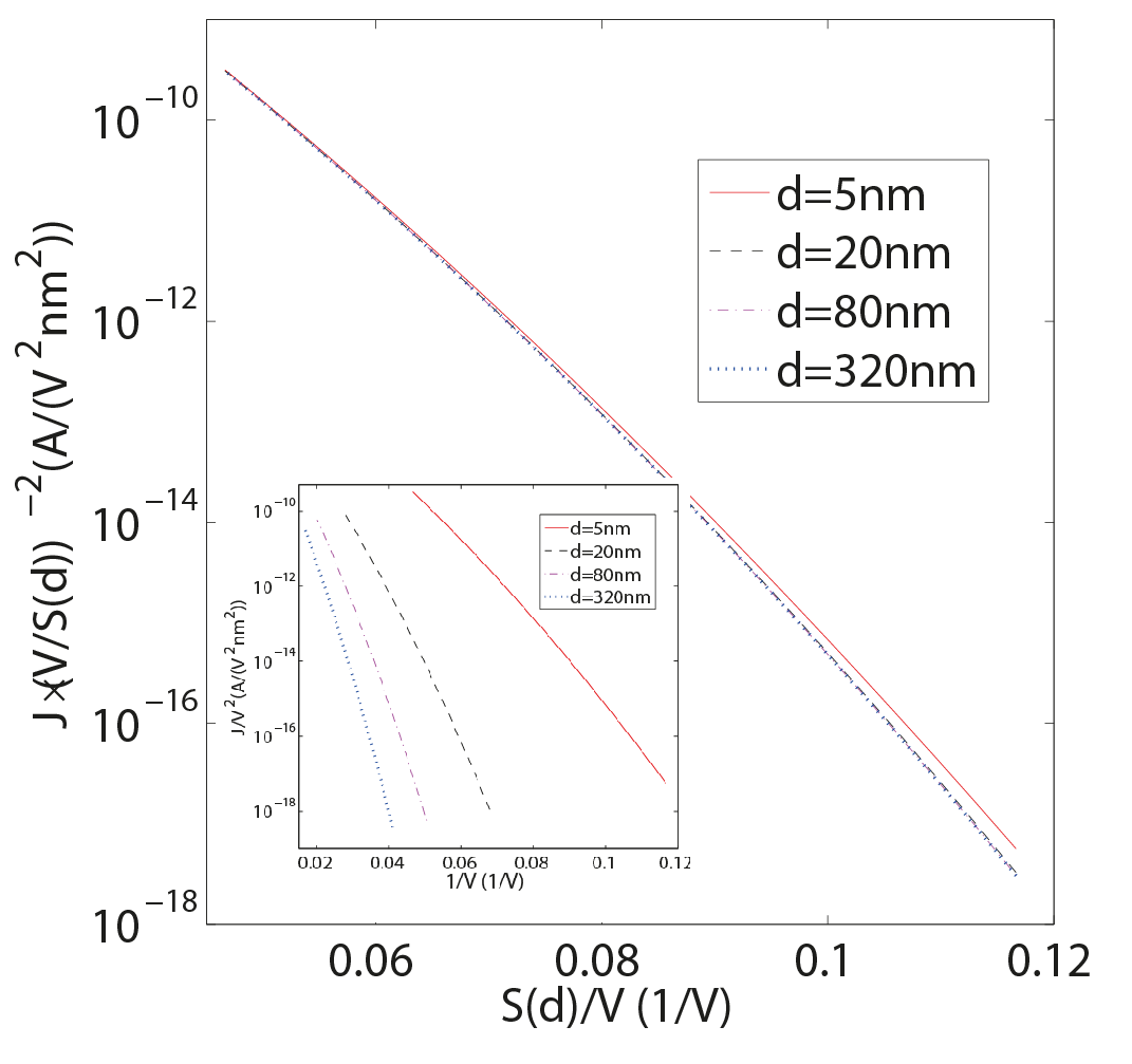
Fig. 3: Scaling properties of NFESEM voltage-current (I-V) characteristics.Main figure: scaled I-V curve, Inset: I-V curves for different d |
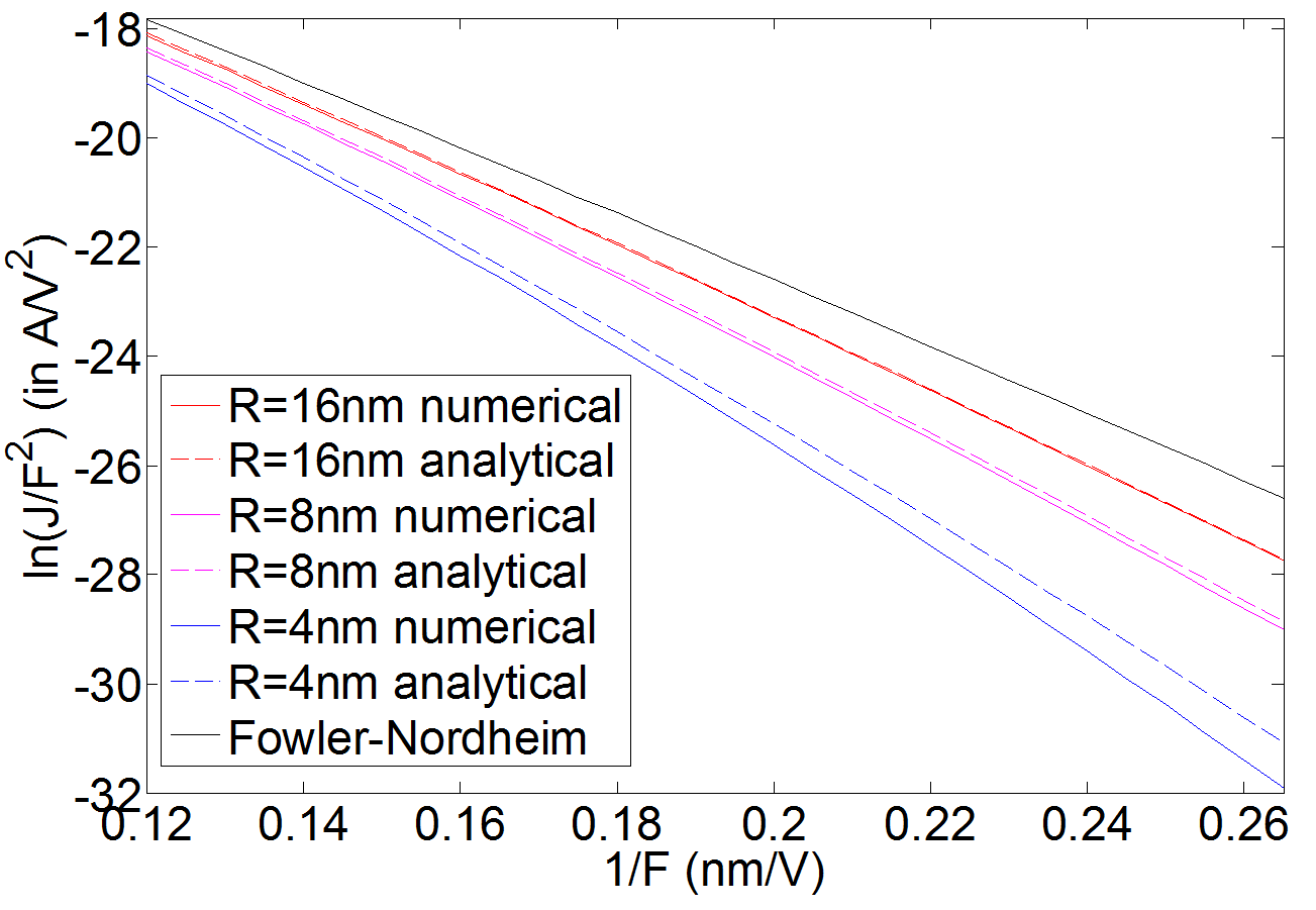
Fig. 4: Comparison of Fowler-Nordheim plots calculated by our compact generalized FN equation and those obtained by ab initio WKB calculations. |