IT-4-P-3166 Combined EDS and WDS analysis of thin specimens with high spatial and energy resolution in the scanning electron microscope
X-ray analysis of bulk samples by energy-dispersive x-ray spectrometry (EDS) in a scanning electron microscope (SEM) is widely used to gain chemical information of materials. The combination of EDS and bulk samples is limited by the low energy resolution of EDS, the associated high detection limit and the low spatial resolution due to the interaction volume of the electrons which is correlated to the beam energy used. A wavelength-dispersive spectrometer (WDS) can increase the energy resolution dramatically. An improvement of the spatial resolution can be obtained by use of very thin samples (less than 50 nm). The combination of EDS, WDS and thin specimens improves the spatial and energy resolution and detection limits and keeps the analysis time down.
All investigations were performed on a Zeiss Ultra 55 equipped with a 10 mm2 Si(Li)–EDS detector and a parallel beam WDS detector with a multi capillary optics from EDAX. Thin specimens were prepared by ion milling with a FIB.
In order to minimize shadowing effects a special sample holder was designed (see Fig. 1). With this sample holder a linescan across a FIB-lamella from a semiconductor device (see Figure 2a) was performed by EDS and WDS. The resulting intensities of the Ti-K peak recorded with both EDS (grey) and WDS (dark grey) are shown in Figure 2b (dwell time 1000ms for EDS and 2000ms for WDS). This Figure demonstrates that the x-ray intensities for both EDS and WDS are sufficiently high for the x-ray analysis of thin specimens. Figures 2c and 2d demonstrate the benefit of the high energy resolution of WDS. Whereas the signal of the W-M line recorded with EDS runs quite similar to that of the Si-K line, WDS clearly proves that in the region with high Si content no W is present.
A FIB-lamella of a circuit board with a 40 nm Au layer followed by a 14 nm Pd layer was analyzed by EDS to validate the improvement of the spatial resolution of x-ray analysis by investigating thin instead of bulk specimens (see Figure 3a). The linescan across these two layers is plotted in Figure 3b. This Figure proves that both layers can be detected separately by x-ray analysis. As a Lorentz distribution was the best fit to the scan of the Pd intensity its half width was used as a measure for the thickness of the Pd layer. It gave a value of 15 nm which is close to the value obtained by the electron image
I would like to thank the FFG for the financial support (Project number: 825165)
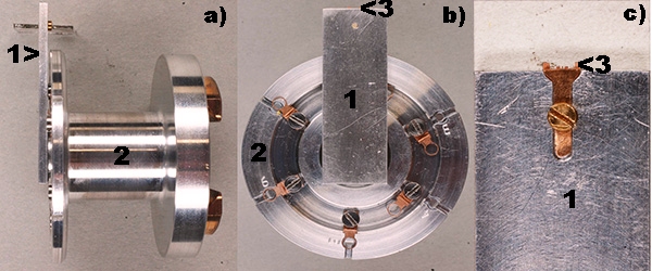
Fig. 1: Modified specimen holder, a) side view b) top view c) bottom view of the optimized holder; 1: optimized holder, 2: original Zeiss STEM holder, 3: FIB-lamella |

Fig. 2: X-ray linescans across a semiconductor structure, a) BSE image with linescan marked (image width: 800 nm) , b) EDS (grey) and WDS (dark grey) signal of the Ti-K line c) EDS and WDS signal of the Si-K line, d) EDS and WDS signal of the W-M line; abscissa: distance in microns, ordinate: number of x-rays. |
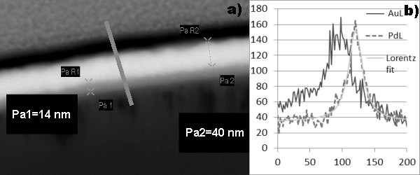
Fig. 3: X-ray linescan across a circuit board, a) BSE image with linescan marked (image width: 380 nm), b) EDS signal of Au-L line (dark grey) and Pd-L line (dashed line grey), light grey the Lorentz fit to the Pd scan; abscissa: distance in nanometre, ordinate: number of x-rays. |
|