IT-5-O-3165 3D EDX in SEM and TEM: common problems and common solutions
Energy dispersive X-ray spectrometry (EDS) has recently seen a step forward with the introduction of silicon drift (SDD) detectors for both SEM and TEM. The improvements in speed and detector efficiency have allowed EDS, a traditionally 2D technique, to be extended to 3D. For SEM, focused ion beam (FIB) ‘slice-and-view’ methods can be used. For TEM, tilt series of 2D EDS maps are recorded for reconstruction by back-projection. 3D EDS mapping in both the SEM and TEM faces acquisition and processing challenges, such as partial detector shadowing, detection of spurious X-ray and high level of noise. In this paper we explore which problems are common to both techniques as well as proposing common solutions. To compare the two techniques, samples of Ni-based superalloy are investigated with complex structures ranging from microns to nanometers (see figure 1) and containing more than 10 elements (see figure 2).
For 3D experiments, the acquisition time per spectrum is often reduced, to cover a large volume or to acquire a sufficient number of tilt images, in a reasonable time. The set of data contains millions of noisy spectra characterizing only a limited set of chemical phases. This is a favorable case for a multivariate statistical approach, such as principal component analysis (PCA), and, as shown in figure 3, an important reduction of noise can be obtained with this technique. However, such statistical approaches need to be used with care, especially with data containing few counts per channel. Alternative PCA algorithms and pre-processing methods will be explored. Before quantification, the X-ray line intensities are extracted from each EDS spectrum. The involved processing steps are similar for SEM and TEM. Due to the relatively low energy resolution of the EDS detector, X-ray lines often overlap, as observed in figure 2 for Hf Mα and Ta Mα. Moreover, the background needs to be subtracted. Given the high level of noise in SEM and TEM datasets, accurate intensity extraction is challenging. Different processing strategies based on curve fitting will be discussed.
For 3D EDS in SEM and TEM, other signals may be recorded simultaneously, such as secondary electron (SE) for SEM or energy loss spectra for TEM. This opens the way for new processing methods benefiting from complementary signals. For instance, SE images can be used to improve the spatial resolution of the segmentation obtained with the EDS map [1]. In order to facilitate the interactive data analysis of these complex multi-dimensional datasets, HyperSpy [2] a free, open-source and open-development software package, has been extended to EDS data for SEM and TEM.
1. P. Burdet, J. Vannod, A. Hessler-Wyser, M. Rappaz, M. Cantoni, Acta Materialia 61 (2013) 3090–3098
2. http://hyperspy.org
The research leading to these results has received funding from the European Research Council under the European Union's Seventh Framework Programme (FP7/2007-2013) /ERC grant agreement 291522-3DIMAGE. SAC and PAM acknowledge financial support from Rolls-Royce plc.
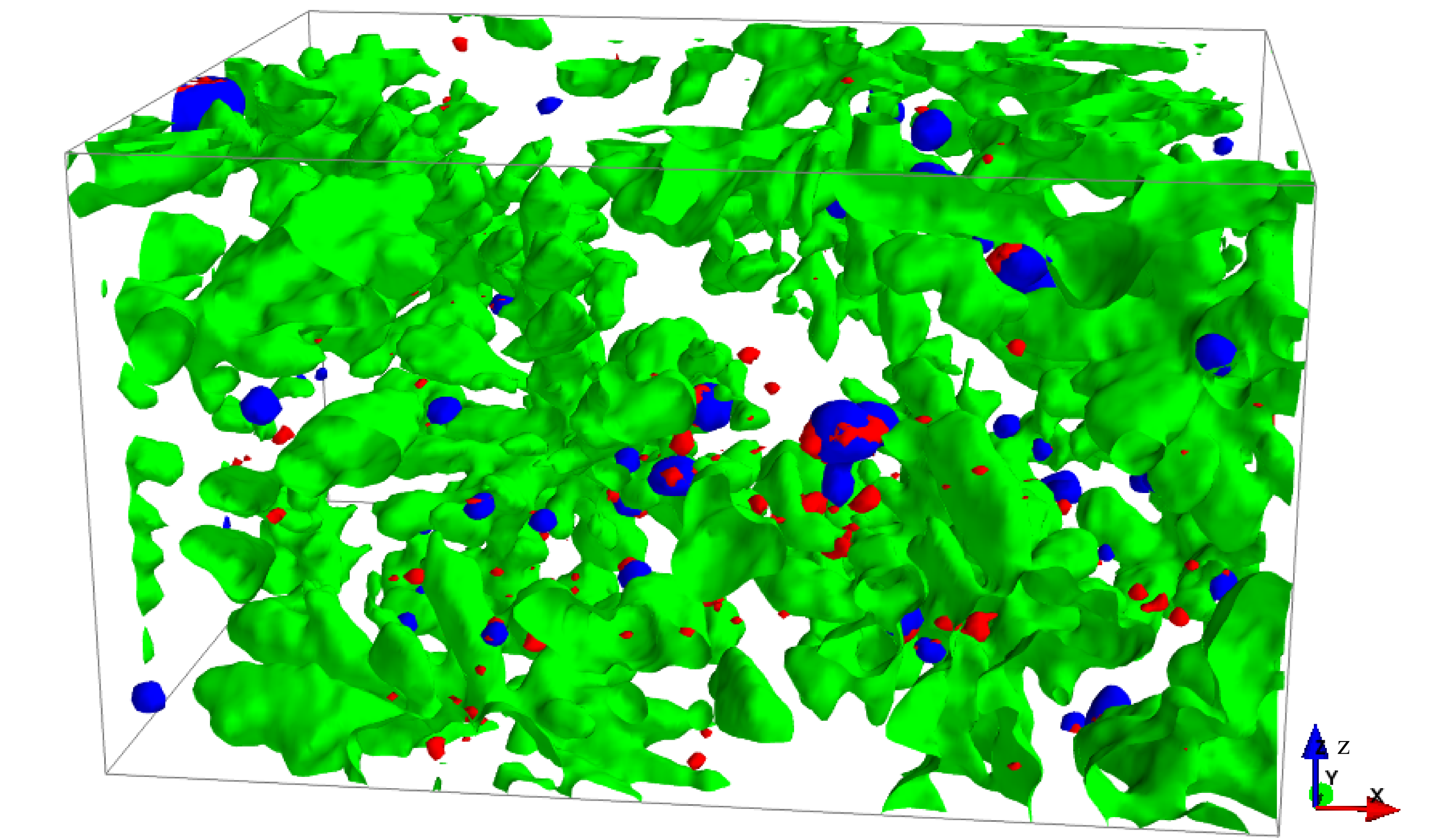
Fig. 1: 3D SEM-EDS reconstruction of the sample of Ni-based superalloy. The green volume shows the Ni rich γ’ phase, red show the Hf rich phase and blue the Ta rich phase. The bounding box measures 12.8 µm x 11.2 µm x 6.3 µm. |
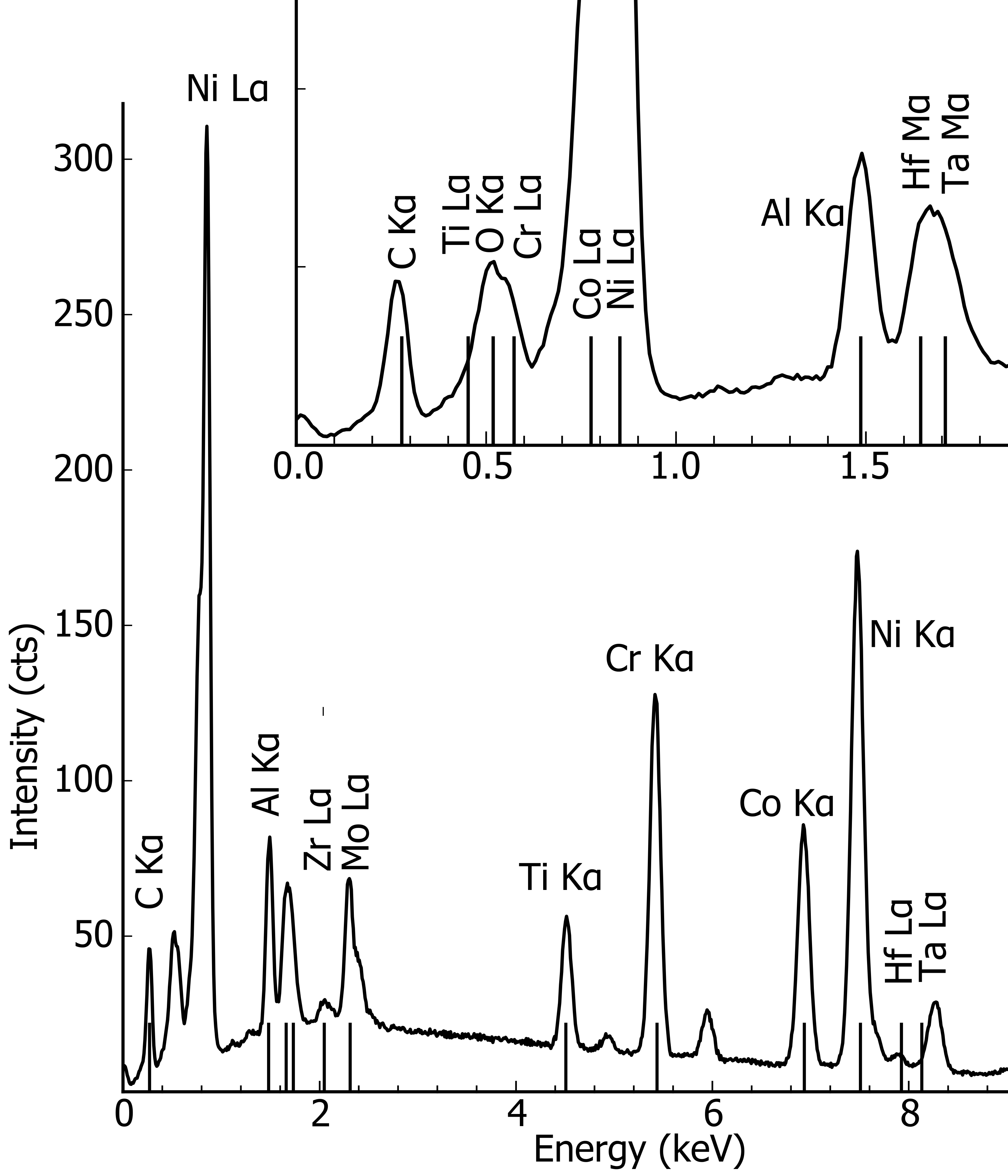
Fig. 2: Characteristic SEM-EDS spectrum acquired from a sample of Ni-based superalloy. The main lines excited at 15 kV are indicated. The inset shows a magnified picture of the low energy lines. |
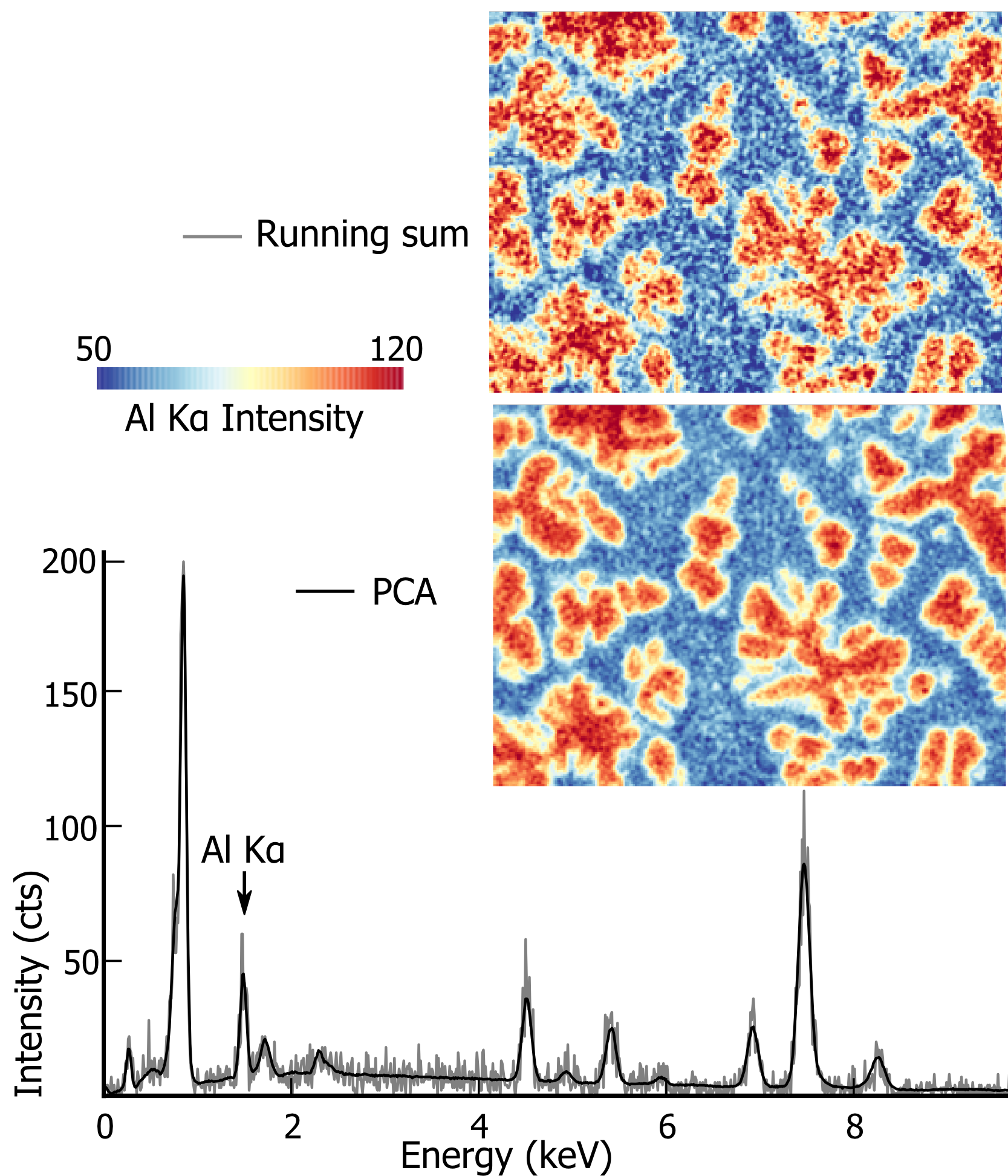
Fig. 3: Denoising a SEM-EDS spectrum with PCA. A running sum is used prior to the PCA. |
|