IT-11-P-3140 Electron Beam induced Currents in GaN p-n Junctions
Off-axis electron holography (EH) is a unique approach for analyzing potential variation down to nanometer scale. In absence of magnetic fields and in kinematical diffraction condition, the phase modulation is proportional to the potential (sum of mean inner potential and built-in potential Vpn) and the specimen thickness. However, quantitative measurement of Vpn in GaN shows a huge deviation with the theoretical value. Additionally, it seems that the hypothetical “dead layer” on both surfaces affected by focused ion beam (FIB) preparation is not the only reason for the discrepancy since the measured Vpn from the bulk (n-GaN)/shell (p-GaN) geometry of the GaN p-n junction is not affected by the FIB preparation [1].
In this study, we assess the influence of the electron beam on the measured Vpn at GaN p-n junctions. Two GaN p-n junctions of comparable dopant concentration were prepared by FIB. Thereby, a needle-like shape geometry is deliberately chosen to ensure that the whole specimen is illuminated during the experiment [2]. Moreover, a defined path of the induced current arising from electron-hole pair generation and secondary electron emission is provided. Low voltage (5 kV) is applied for the final polishing step to mitigate the surface damaging by FIB.
Fig. 1 shows the FIB milled needle with a sketch of the layer structure. In order to enhance the signal to noise ratio of the phase, series of holograms separately for each illumination intensity were recorded and subsequently averaged. The reconstructed phase depicts a clear phase jump at the p-n junction (Fig. 1 (c)).
Two electron beam induced effects are observed. Firstly, in Fig. 2 the measured Vpn increases with reducing the electron dose rate. This illumination dependency of Vpn can be quantitatively explained by a solar-cell model. Hence, Vpn = Vpn, expected – Vbias is fitted on the data set, where Vpn, expected is determined by the doping concentration (sample A: 3.41 V, sample B: 3.43 V), Vbias is the voltage drop across the p-n junction, which is affected by illumination induced currents owing to secondary electron emission and e-h pair generation [3]. Additionally, fluctuation of Vpn is depicted by two needles, which are prepared from a same wafer and with the same FIB preparation steps. However, both needles (I and II) show the same behaviour of Vpn over the electron dose rate. Secondly, beam damage of the specimen is observed in Fig. 3. The Vpn diminishes over a period of time and might converge to a constant value, which is about the half of the initially measured Vpn.
1. S. Yazdi et al., journal of physics: Conf. Ser. 471 (2013), p.012041.
2. A. Lenk, Dissertation, Dresden (2008).
3. S.M. Sze in “Physics of Semiconductor Devices”, 2. Edition, John Wiley & Sons (1981).
This work is carried out within the framework of the DFG collaborative research center SFB787 semiconductor nanophotonics.
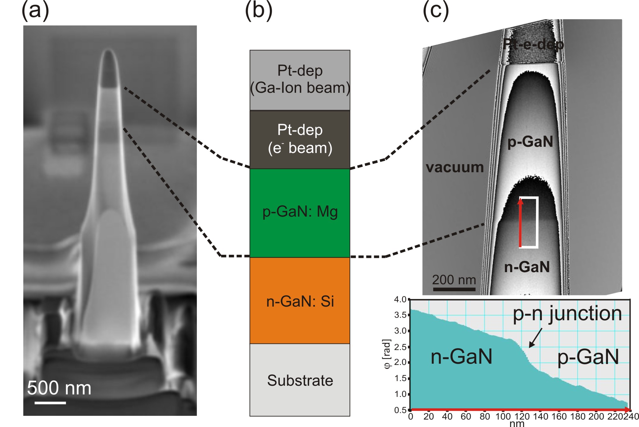
Fig. 1: (a) SEM image of the needle-like shape specimen after FIB preparation. (b) The layer structure of the specimen. (c) The reconstructed phase of (a). The phase jump at the p-n junction due to different doping type is clearly visible. The large-area undulation of the phase change along the specimen is caused by thickness variation. |
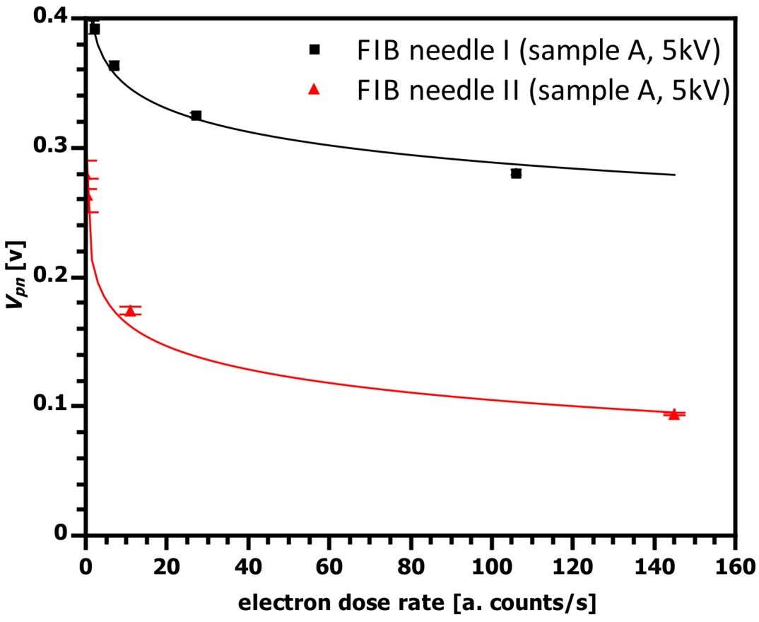
Fig. 2: The measured built-in potential Vpn over the electron dose rate for two needle specimens of sample A (FIB needle I and II). The Vpn is enhanced over roughly 30% by reducing the electron dose rate by a magnitude of 2. |
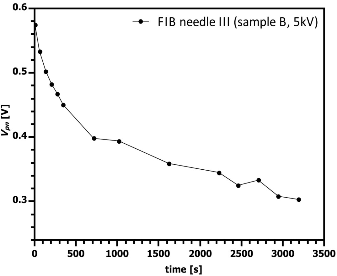
Fig. 3: The Vpn is measured directly after FIB preparation over a period of time (about 1 hour) at sample B. We observe a decrease of Vpn by a factor 2 over time. |
|