IT-7-P-3115 In-situ heating using MEMS devices on FIB/SEM systems
Introduction
Information on the kinetics of microstructural evolution is important in materials science fields like recrystallization, grain growth and phase changes. This requires reliable discrimination of differently oriented crystallites or different crystal phases, coupled with useful spatial resolution, temporal resolution and temperature change rate. Currently available SEMs have spatial resolution below 1 nm, temporal resolution below 10 ms (100 Hz frame rate), but existing heating holders only allow heating bulk samples up to 100°C per minute (~2°C/s). This prohibits experiments like quenching of metals and the long ramping time may cause the sample to change (oxidize, recrystallize) before the temperature range of interest is reached. In addition the backscatter (grain-, phase-) contrast is deteriorated because solid state detectors are blinded by the infrared radiation from the sample.
As a solution to these problems we present a MEMS heating holder [1], [2] in combination with in-situ sample preparation using a DualBeam FIB/SEM.
Sample preparation
A chunk of material is cut with the FIB and attached to the micromanipulator needle using beam-induced deposition (Figure 1a). After lift-out it can be further shaped using the FIB (1b). It is then placed on the MEMS heating holder, fixated with beam-induced deposition and cut loose from the needle (1c).
Ramping rates
The tiny thermal mass of the MEMS heater and sample allow temperature changes of 1000°C in just 50 ms (2·104°C/s) for a Cu sample of 20x50x50 um3 size (including settling to within 20°C, both for heating and cooling).
Imaging
The small heated area of the MEMS heater reduces the infrared radiation sufficiently that solid state detectors such as in-chamber BSE detectors and EBSD cameras can be used at elevated temperatures. Figure 2, for example, shows the melting of gold micro-particles at 1064°C imaged with the solid state BSE detector.
References:
[1] L. Mele et al. “A molybdenum MEMS microhotplate for high-temperature operation”, Sensors & Actuators: A. Physical, 2012 | 188 | 173-180
[2] B. Morana et al. “A silicon carbide MEMS microhotplate for nanomaterial characterization in TEM”, Micro Electro Mechanical Systems (MEMS), 2011 IEEE 24th International Conference on, 23-27 Jan. 2011, 380-383
This work was supported by Technology agency of the Czech Republic, project no. TE01020118 (Competence centre: Electron microscopy).
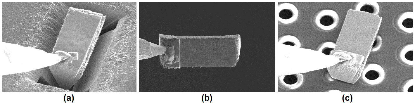
Fig. 1: Figure 1: Sample preparation from bulk sample: extraction using ion beam and manipulator (a); shaping of sample on manipulator needle (b); placement on MEMS heating holder (c). Horizontal field width is 50µm. |
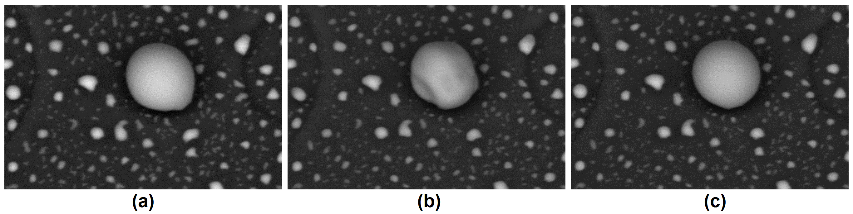
Fig. 2: Figure 2: Solid State Detector BSE imaging of gold particle solidification (a → b) and re-melting (b → c). Horizontal field width is 10µm. |