IT-5-O-3107 Luminescence of structural defects in opto-electronic materials studied by CL-STEM
The cathodoluminescence (CL) signal from opto-electronic materials is a sensitive function of their structural properties. CL mapping in scanning TEM (STEM) mode offers a number of advantages for studying this relationship. The interaction volume of the electron beam has a diameter of a few nm within the TEM lamella or sample, giving the potential for high spatial resolution CL studies (e.g. [1]). Further, the CL signal can be acquired simultaneously with defect contrast images taken with bright-field (BF) or low angle dark-field (LDF) detectors, and atomic number contrast images from a high angle annular dark-field (HAADF) detector. This allows direct correlation of luminescence to structure and defects.
Here we present studies using CL-STEM to probe the effects of structural defects on optical properties. Data are taken using a JEOL 2200FS equipped with the Gatan XiClone CL spectrometer, at 80 keV beam energy to increase CL signal and reduce beam damage. The instrument has BF, LDF, and HAADF STEM detectors; sample holders allow specimen temperatures from 5 K to room temperature. Para-CL spectrum image data are acquired on a liquid nitrogen cooled CCD camera using Gatan Digiscan, typically using a 300 lines/mm grating and sub-pixel scanning for the simultaneously acquired STEM images.
To optimize experimental conditions and to interpret data it is important to characterize the sample-instrument system. Fig. 1 shows the effects of specimen thickness and temperature on the CL signal of a GaN epilayer prepared for TEM by mechanical wedge polishing. Specimen cooling increases CL signal intensity and also reduces non-radiative recombination at the polished surfaces, so giving luminescence even for 30 nm thick material. Fig. 2 then shows threading dislocations in an InGaN quantum well (QW) on a GaN substrate. Some dislocations demonstrate modulations in wavelength that could correlate to In enrichment and depletion in the strain fields around their core [2]. Fig. 3 instead shows data taken from a GaN nanowire that contains stacking faults (SFs) on the basal plane [3]. The spatial correlation of SFs to the near-bandgap (NBE) and sub-bandgap (SBE) emission is complex, demanding further investigation, while midgap states generate a diffuse background. The observation of Fabry-Pérot resonator effects for CL in the TEM lamella will also be discussed. Together these results illustrate the great potential of CL-STEM for investigating the structure-optical domain.
[1] Zagonel et al., Nano Lett. 11, 2011, 568
[2] Mouti et al., PRB 83, 2011, 195309
[3] Schuster et al., Nano Lett. 12, 2012, 2199
The Competence Centre for Materials Science and Technology (CCMX) is acknowledged for CL funding, and Anas Mouti of ORNL for earlier works with the CL-STEM system.
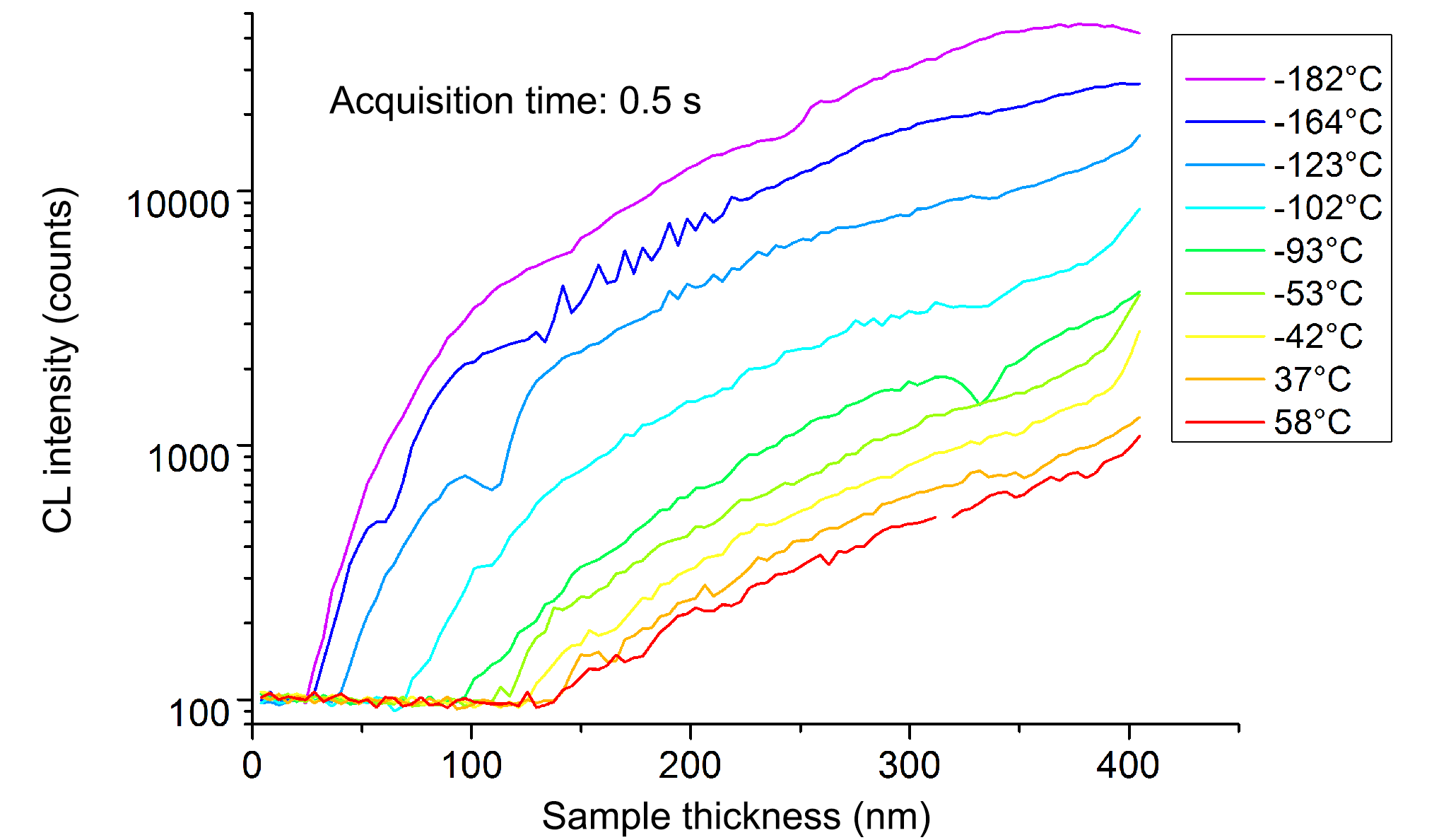
Fig. 1: CL intensity of the GaN peak as a function of thickness at different temperatures. Extracted from CL line scans taken on a GaN epilayer sample with a wedge shape. Thicknesses estimated by electron energy-loss spectroscopy. |
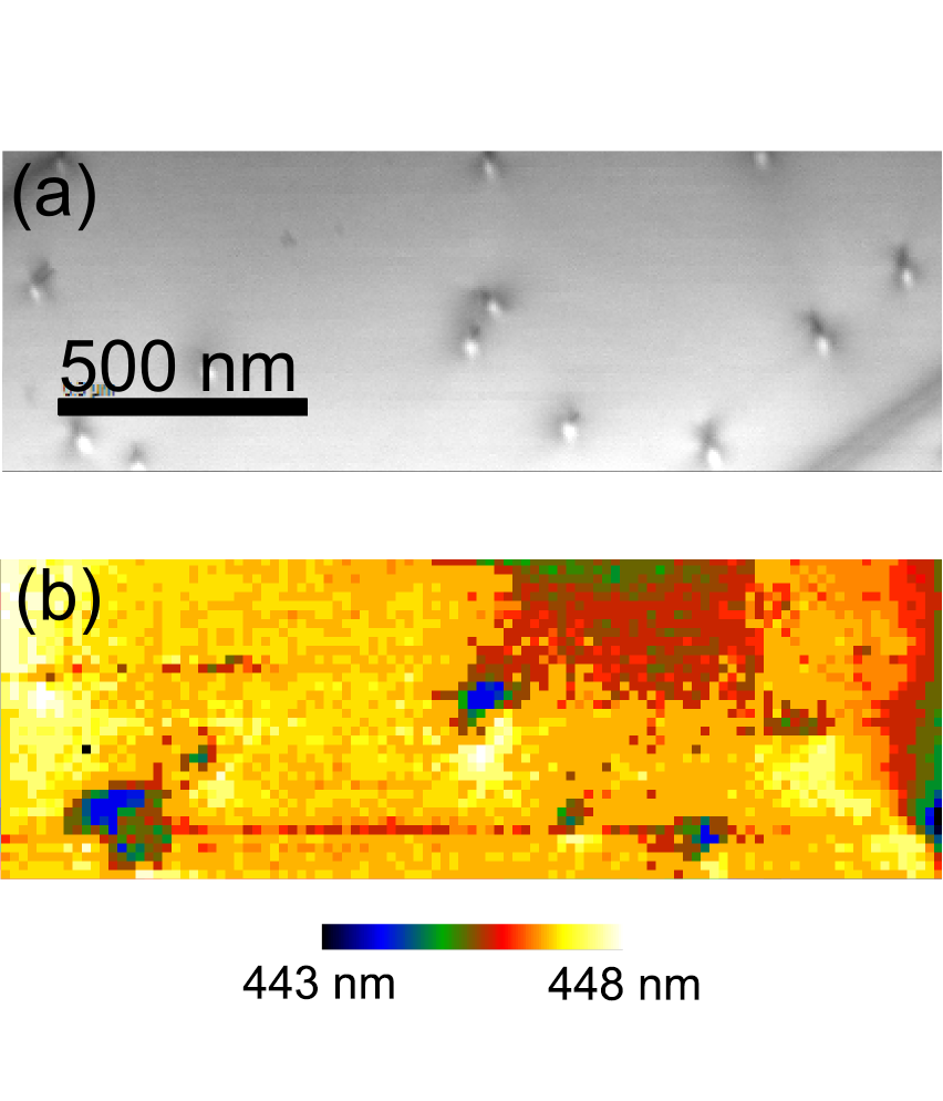
Fig. 2: (a) BF STEM image of a single InGaN QW on GaN substrate in plan view with threading dislocations coming to the surface. (b) Map of the wavelength of the QW peak (colour scale shown below). A butterfly shape is visible around some of the dislocations with emission blue-shifted on one side and red-shifted on the other. |
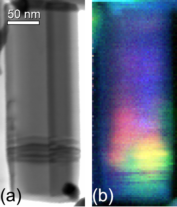
Fig. 3: (a) BF STEM image and (b) RGB CL map of different emission bands for a GaN nanowire (red: NBE; green: SBE; blue: midgap states). While the planar defects in the nanowire have an influence on CL emission, there is not a direct spatial correlation between the two. |
|