IT-7-P-3015 In situ applications of quantitative magnetic TEM imaging in magnetic nanostructures
Magnetic imaging TEM techniques such as Lorentz Microscopy (LM) and Electron Holography (EH) are powerful tools to extract valuable quantitative information with nanometer-range resolution on the local magnetic states of nanomaterials. We usually study magnetic nanostructures at room temperature and at remanent state, but the use of special TEM specimen holders and/or set-ups opens the possibility to explore in situ the evolution of magnetization states upon the application of external stimuli such as temperature changes, magnetic fields or electric currents.
In this work, we present different applications of in situ LM and EH experiments under different scenarios: the in situ application of magnetic field with a calibrated objective lens is achieved by a smart control of the tilt angles of a double-tilt holder. A mathematical procedure has been developed to determine and/or quantify the in-plane component of the applied magnetic field. This capability is illustrated with two applications: the analysis of the domain conduit properties of magnetic nanowires by measuring the nucleation and propagation (depinning) fields [1], as shown in Figure 1(a); and the accurate determination of the magnetic hysteresis loops in nanoscaled magnetic tunnel junctions (MTJs) shown in Figure 2(b), where the different orientation of the magnetic induction component normal to the electron beam with respect to the induction in the sample’s plane can be quantified and corrected [2]. The potential of cryogenic conditions to study magnetism in nanostructures (down 100 K) is demonstrated by the investigation of the magnetic properties of La0.67Ca0.33MnO3 manganite thin films [2] and the strain effects on the suppressed ferromagnetism observed, an example of this characterization is displayed in Figure 2. Finally, the use of a dedicated two-contact TEM holder for the injection of spin-polarized currents in Py nanowires, illustrated in Figure 3, is applied to the investigation of current-induced domain wall manipulation phenomena.
[1] L. A. Rodríguez et al., Appl. Phys. Lett. 102, 022418 (2013).
[2] L. A. Rodríguez et al., Ultramicroscopy 134, 144-154, (2013).
This work was supported by the Spanish MINECO Projects MAT2009-08771, MAT2011-28532-C03-02 and MAT2011-28532-C03-03. The authors acknowledge the European Union under the Seventh Framework Programme under a contract for an Integrated Infrastructure Initiative Reference 312483-ESTEEM2.
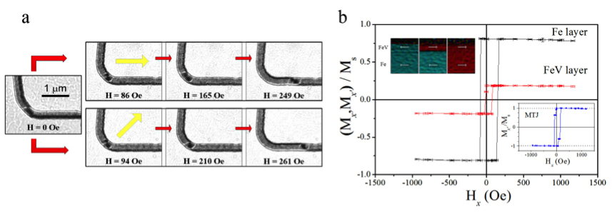
Fig. 1: (a) Depinning DW processes in CoFe nanowires by application of parallel and transversal magnetic fields (yellow arrows indicate the magnetic field directions), (b) Hysteresis loops in a Fe/MgO/FeV MTJ. |

Fig. 2: Amplitude, magnetic phase shift (MAG) and magnetic flux (B) recorded by Electron Holography at low temperature (100 K) of (a) full magnetized and (b) with a superficial non-ferromagnetic layer (NFL) epitaxial La0.67Ca0.33MnO3 thin films grown on SrTiO3 substrates. |
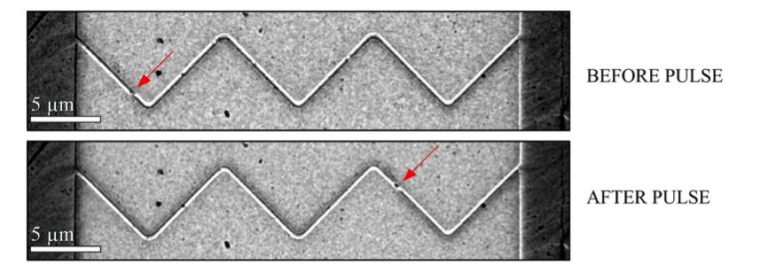
Fig. 3: Defocused LM images recorded before and after injecting an electrical current pulse of an amplitude of 1 mA and a duration of 100 μs. Red arrows point a domain wall which is propagated after the pulse. |
|