IT-4-P-3005 Microstructural characterization of metallic materials using advanced SEM techniques
The development of advanced materials is inseparably connected with detailed knowledge of the relationship between microstructure and mechanical properties. Traditional high-voltage scanning electron microscopy (SEM) is one of the most commonly used techniques for microstructure analysis, though it may be insufficient particularly for the characterization of advanced materials exhibiting a complex microstructure.
The benefits of using slow electrons have been described in several articles [e.g. 1,2]. Experiments have been performed with a XHR SEM Magellan 400L (FEI Company) equipped with two detectors for secondary electrons (SE), an Everhart Thornley detector and an in-lens TLD detector, and solid-state BSE detector (CBS) located below the pole piece. This microscope can also be operated in the beam deceleration (BD) mode [3]. The field of the BD not only decelerates the primary electrons, but also accelerates the emitted (signal) electrons towards the detector. Furthermore, high-angle backscattered electrons (BSE) are also collimated towards the optical axis and are detected. These electrons carry, first and foremost, crystal orientation contrast. SE and low-angle BSE can be detected by the TLD detector located inside the objective lens. Angle-resolved detection of BSE is performed using a CBS detector divided into four concentric segments.
Fig. 1 shows the dependence of material contrast between BN precipitates, Laves phase and matrix on the landing energy and increasing of contrast between differently oriented areas in advanced creep resistant steel COST CB2. The presence of BN precipitates and Laves phase has been verified by EDX analysis. The prospect of angular separation of BSE is shown in Fig. 2. The trajectories of signal electrons were simulated in EOD software [4]. It is clearly visible that the low-angle BSE detected by means of the segments closest to the optical axis (S1 and S2) provide information about the chemical composition of the specimen. Segment S3 offers high crystallographic contrast, and material contrast between Laves phase and matrix is entirely suppressed. The final segment S4 exhibits topographic contrast due to the detection of electrons emitted under very high angles from the optical axis, which are products of the interaction of the primary electrons with surface irregularities.
[1] L. Raimer: Image formation in low-voltage SEM. SPIE Press (1993)
[2] I. Mullerova and L. Frank: Scanning low-energy electron microscopy. Adv. Imag. Elect. Phys., Vol. 128 (2003)
[3] Product specification. XHR SEM Magellan 400L. FEI Company
[4] J. Zlamal and B. Lencova: Nucl. Instr. Meth. Phys. Res. A, Vol. 645 (2011)
This work was supported by project no. TE0120118 (Competence Center: Electron Microscopy). The author Šárka Mikmeková is sponsored by an FEI Company Scholarship.
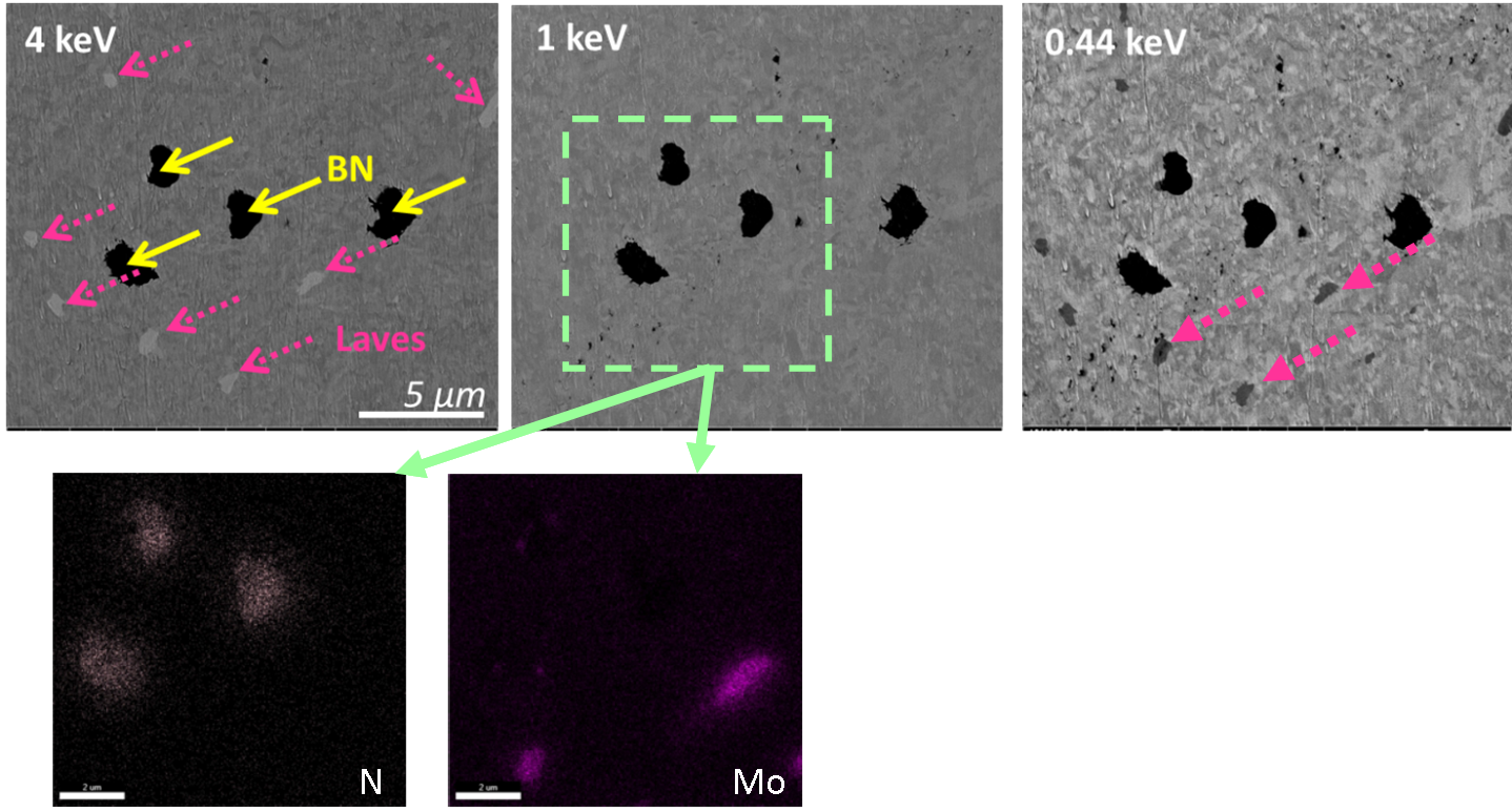
Fig. 1: Fig. 1 The same field of view imaged at 4 keV, 1 keV and 0.44 keV landing energy using the DB mode (specimen bias – 4 kV in all cases), together with corresponding EDX maps of N and Mo distribution. |
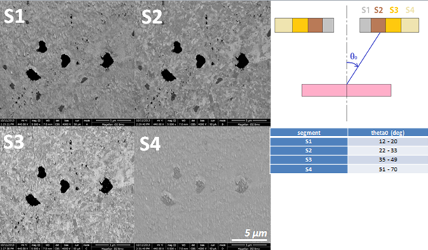
Fig. 2: Fig. 2 Micrographs obtained at 440 eV landing energy (specimen bias – 4 kV) by means of separated parts of the CBS detector, together with information about detected angles by each segment. |