IT-5-P-2960 Advanced EELS Spectrum Imaging of RRAM Devices: Chemical State and Three-Dimensional Element Mapping
Resistance random access memory (RRAM) has become more and more important because of its high writing/reading speed and low power consumption in the field of non-volatile memory applications. The understanding of the programming and reliability mechanisms in RRAM devices requires a detailed characterization of the microstructure, chemical bonding and element distribution. The scanning-transmission electron microscopy- electron energy loss spectroscopy (STEM-EELS) collects spectrum in every single probe position and form a spectrum image (SI) while it represents a powerful tool to link the physical and chemical structure of RRAM devices to their macroscopic properties. The research focuses on the recent development of STEM-EELS-SI,[1-2] including sub-angstrom resolution (≤ 1 Å), mapping chemical bonding and chemical 3D tomography, which can be performed because of the improvement of modern aberration-correcting technology. The STEM-EELS-SI tomography utilized a rotation holder and pillar-shaped specimen to allow the STEM mode angular dark field (ADF) and EELS spectrum images to be recorded over a complete 180o rotation to minimize the missing wedge artifacts. The fine structure of EELS SI was analyzed with multiple linear least-squares (MLLS) fitting to map out the relative intensities associated with a number of chemical states of core loss edges. During the acquisition of EELS-SI, the fast (electrostatic) shutter of EELS spectrometer was used while it provided high quality spectra at a dose low enough to prevent damage and chemical decomposition of the specimen. Finally, the principal component analysis (PCA) was applied and low signal to noise of the raw data was acceptable, further increase the throughput of EELS-SI. The findings of observed elements re-distribution have implications for the transition mechanism between the high resistance state (HRS) and low resistance state (LRS) driven by the external electric field. The filaments (conductive region) can be characterized by chemical mapping extracted from EELS-SI at the nanometer scale. It seems, then, that the oxygen-deficient and metal clusters play an important role in the resistive switching mechanism. Two kinds of filaments are observed via the EELS spectrum image analysis. This research is to establish analytic TEM analysis techniques for advanced devices, which can be applied to the RRAM、MRAM storage、IC and flash memory industry.
Reference:
1. K. Lepinay, F. Loruta, R. Pantel, and T. Epicier, Micro, 47, 43-49, 2013.
2. K. Jarausch, P. Thomas, D. N. Leonard, R. Twesten, C. R. Booth, Ultramicroscopy, 109, 326-337, 2009.
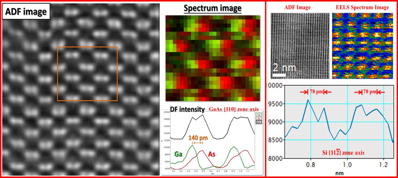
Fig. 1: sub-angstrom resolution EELS spectrum images (materials: GaAs and Si) |
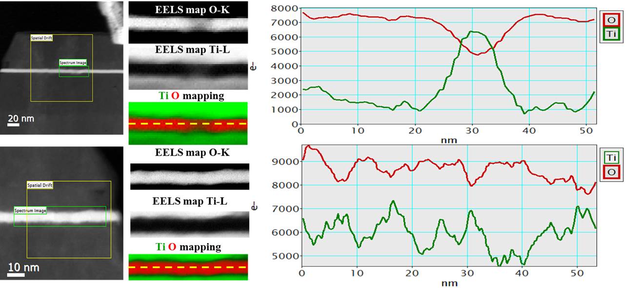
Fig. 2: EELS spectrum images revealing the mechanism of filament formation in RRAM devices |
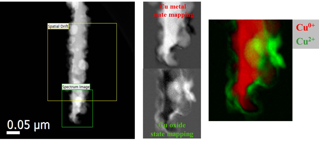
Fig. 3: chemical state mapping of copper oxide nano-materials using EELS spectrum images |
|