IT-5-P-2909 Advantages of Combining EDS and Energy Filtered STEM Diffraction at Atomic Level
Very recently a technique called STEM Diffraction has been used to collect the entire diffraction pattern (DP) in STEM mode at each probe position and store it in a data-cube [1]. The advantage is that every feature in the DP can now be recorded at each probe position. In this way it is possible to take advantage of the wealth of information present in the DP and have the spatial resolution offered by the STEM probe. In addition, virtual STEM detectors can be created and images can be generated by integrating the intensity of the DP over an appropriate angular distribution that depends on the particular element being imaged. For instance, light elements show high contrast within a narrow angular distribution at low angle in the DP and this is analogous to medium annular bright field (MaBF) imaging (2).
Here we propose an alternative approach where EDS spectra and DPs are acquired simultaneously at atomic level. DPs are acquired using the camera attached to an energy filter in EFTEM mode with a 10eV slit inserted in order to remove the inelastic scattering effects that blur the contrast in the DP. EDS can be used to generate elemental distribution maps. However, even with the use of the latest generation of detectors, EDS is not sensitive towards light elements especially when imaged at atomic level. STEM Diffraction can be used to generate and deliver all the additional structural information present in the DP and also images of atomic columns containing only light elements by integrating over low angular distributions in the DP.
As example, a EDS/(energy filtered) STEM Diffraction dataset was taken at atomic level across a SrTiO3/LaFeO3 (STO)/(LFO) interface as shown in Figure 1. Figures 2 show DPs extracted from the Ti +O, Sr and pure O columns respectively. Features in the DP at every angular distribution are different across each atomic column and can be used to generate additional structural information. Figure 3 shows color maps of Sr in red, Ti in green, La in amber, Fe in light blue acquired using EDS while pure O columns in blue obtained by integrating the signal over 0 – 8mrad angular range in the DP. It is quite interesting to notice how the position of pure O columns is slightly asymmetric in the LFO region compared to the STO. This might be due to the presence of strain at the interface whose effects can create some crystal distortion in the LFO region. This paper will show other examples and discuss the advantages of this combined EDS/STEM Diffraction approach.
References:
1) Okunishi E. et al., Micron 43 (2012) 538-544
2)Findlay S.D. et al., Ultramicroscopy 136 (2014) 31-41
The authors would like to thank IBM for providing the TEM samples and access to their microscope installation
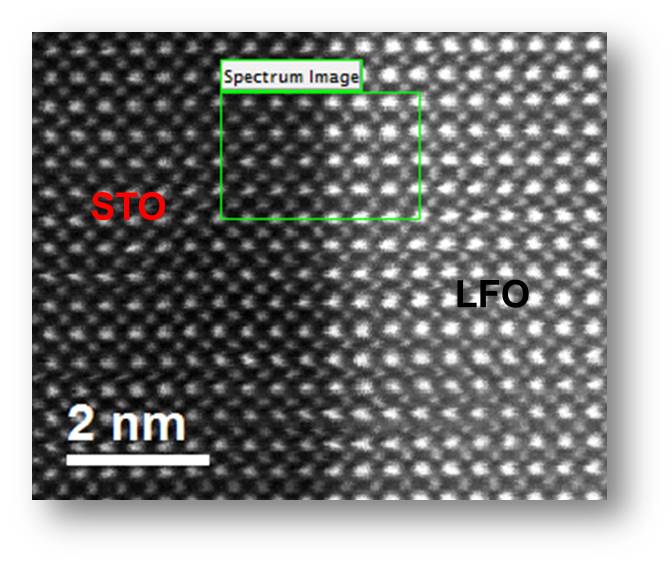
Fig. 1: ADF STEM survey image. The green box is the area where the beam was scanned for the acquisition of the EDS/STEM Diffraction dataset. According to the image the interface STO/LFO seems quite nice and abrupt. |
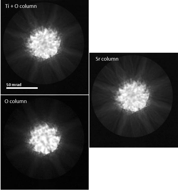
Fig. 2: Series of Diffraction patterns from the STO region and extrcated from the Ti + O, Sr and pure O atomic columns. It is interesting to notice how features in the diffraction pattern at low and high angular range are different in each atomic column |
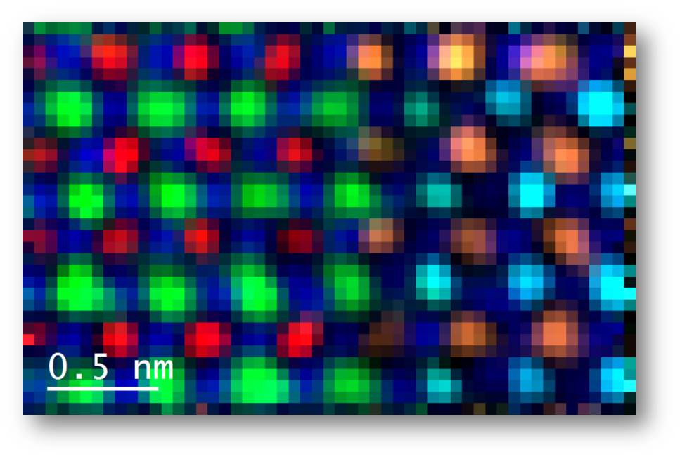
Fig. 3: Elemental color maps of Sr in red, Ti in green, La in amber and Fe in light blue obtained using EDS and pure O atomic columns in blue obtained selecting a 0 - 8mrad angular distribution in the diffraction pattern. The position of the pure O atomic column appears to be slightly asymmetric in the LFO area compared to the STO. |
|