IT-2-O-2885 Three-dimensional location of a single dopant with atomic precision by aberration-corrected ADF STEM
Impurity doping is the key technology for enhancing physical and chemical properties in semiconductors. These functional dopants usually take the form of isolated single atoms, and the materials properties have strong sensitivities to the doping concentration, spatial distribution and three-dimensional location of the dopants. The recent development of aberration-corrected electron microscopy has allowed the determination of the two-dimensional spatial distribution of single dopants with atomic spatial resolution. However, this resolution has been achieved only in the lateral directions, and the last dimension, depth, has not yet achieved atomic resolution.
Here we use quantitative annular-dark field scanning transmission electron microscopy (ADF STEM)[1] to directly visualize isolated single Ce dopants accommodated in bulk w-AlN single crystals[2], exhibiting strong visible-light photo-luminescence. Through combining with frozen phonon image simulations, we determine the three-dimensional location of the Ce dopant with single atomic-layer precision in depth[3].
On the basis of the mean signal value comparison between the experiment and the simulations, we estimate the number of atoms per column, and the atomic-resolution thickness map is shown in Figure 1a. During sequential acquisition, we observed a single Ce dopant jump from X to Y through the interstitial site (Figure 1b-d). For the two columns of X and Y, we performed image simulations of all the possible dopant configurations in depth. In the thicker specimen, it may be difficult to uniquely determine the depth location of a single dopant owing to strong dynamical intensity oscillation. To overcome this issue, we implemented multi-component analysis such as mean signal value, maximum peak intensity and profile fitting. As shown in Fig. 1e, the experimental profile at atom X is well matched with that of the simulation of dopant location to a 9 unit-cell depth. And similarly, atom Y is located to a depth of 8 unit-cells. To develop more general method, we also analyze the same data set with Bayesian statistical model, which does not require a priori knowledge of the number of atoms. And we obtained the same depth locations of Ce dopant. By tracking a single dopant, we could begin to determine the three-dimensional atom diffusion path within bulk materials.
References
[1] R. Ishikawa, A.R. Lupini, S.D. Findlay and S.J. Pennycook, Microsc. Microanal. 20, 99 (2014).
[2] R. Ishikawa, et al., Sci. Rep. 4 3778 (2014).
[3] R. Ishikawa, A.R. Lupini, S.D. Findlay, T. Taniguchi and S.J. Pennycook, Nano Lett., (2014) in press.
R.I. acknowledges support from JSPS Postdoctoral Fellowship. A.R.L. acknowledges support by the U.S. DOE. S.D.F. acknowledges support under the Discovery Projects funding scheme of the Australian Research Council (Project No. DP110101570). T.T. acknowledges support by a Grant-in-Aid for Scientific Research on Innovative Areas "Nano Informatics" (Grant No. 25106006) from JSPS.
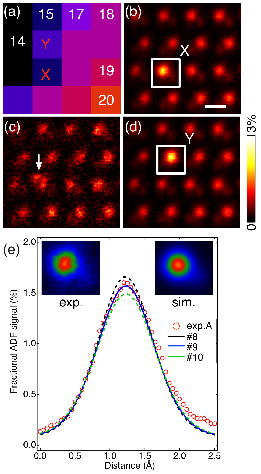
Fig. 1: Figure 1. Sequentially acquired Z-contrast images of w-AlN viewed along the [11-20] direction, (a) atomic-resolution thickness map, (b) averaged over frames of 1-19, (c) frame 20, (d) frames of 21-40. (e) Z-contrast profiles obtained from atom X (exp.) and the simulations of Ce locations to 8, 9, 10-unit cells. |