IT-7-O-2818 Cold-field emission and charge measurements of a carbon cone nanotip studied by in situ electron holography
The cold-field emission gun (C-FEG) is the brightest electron source available, and also exhibits the smallest energy spread [1]. This technology has been greatly improved over the years concerning the electron optics and the vacuum, but the same cathode materials are still in use [2]. We have recently developed a new C-FEG source using a carbon cone nanotip (CCnT) mounted on a standard tungsten cathode using a focused ion beam (FIB) [3]. This source exhibits very good spatial coherence properties, which could be useful for electron interferometry applications [4].
Here, we have inserted a CCnT inside an in situ biasing transmission electron microscope (TEM) sample holder (Nanofactory Instruments) incorporating a nanomanipulator, in order to approach the CCnT towards a Au-anode plate (Fig. 1). We then ramped up the voltage between the nanotip and the anode from 0 to 95 V until the electric field around the tip was strong enough to allow the electrons to tunnel through the barrier and a field emission current could be recorded.
We have previously reported of how quantitative information of the local electric field of the CCnT (Eloc = 2.55 V/nm at the onset of field emission at 80 V) could be obtained by using off-axis electron holography and finite element method (FEM) modeling (Fig. 3 b)). By combining this with the Fowler-Nordheim equation [5], also the work function of the CCnT (Φ = 4.8 ± 0.3 eV) could be found [6].
Knowing the local electric field and the work function, the study has been expanded further to focus on the accumulation of charges on the CCnT before, at and after the onset of field emission. This was done with a technique that we recently have developed [7], which quantitatively measures the number of charges by applying the elegance and power of Gauss’s Law to electron holograms (Fig. 2). It provides a direct measurement of the charge inside a contour integral, with a sensitivity of one unit of charge.
The number of accumulated charges and the charge density on different places on the tip has been determined. We will show quantitative charge measurements along the CCnT as a function of applied voltage (Fig. 3 a)). Particularly the charge density at the beginning and during the field emission process provides some remarkable results. We will then discuss the importance of these values.
[1] O. L. Krivanek et al., Advances in Imaging and Electron Physics 153 (2008)
[2] A. V. Crewe et al., Rev. Sci. Instrum. 39 (1968)
[3] F. Houdellier et al., Carbon 50 (2012)
[4] F. Houdellier and M. Monthioux, International Patent Number WO2012035277 (2012)
[5] R. H. Fowler and L. Nordheim, Proceedings of the Royal Society of London 119 (1928)
[6] L. de Knoop et al., Micron, accepted (2014)
[7] C. Gatel et al., Phys. Rev. Lett. 111 (2013)
The authors acknowledge the European Integrated Infrastructure Initiative reference 312483-ESTEEM2 and the French "Investissement d'Avenir" program reference No. ANR-10-EQPX-38-01.
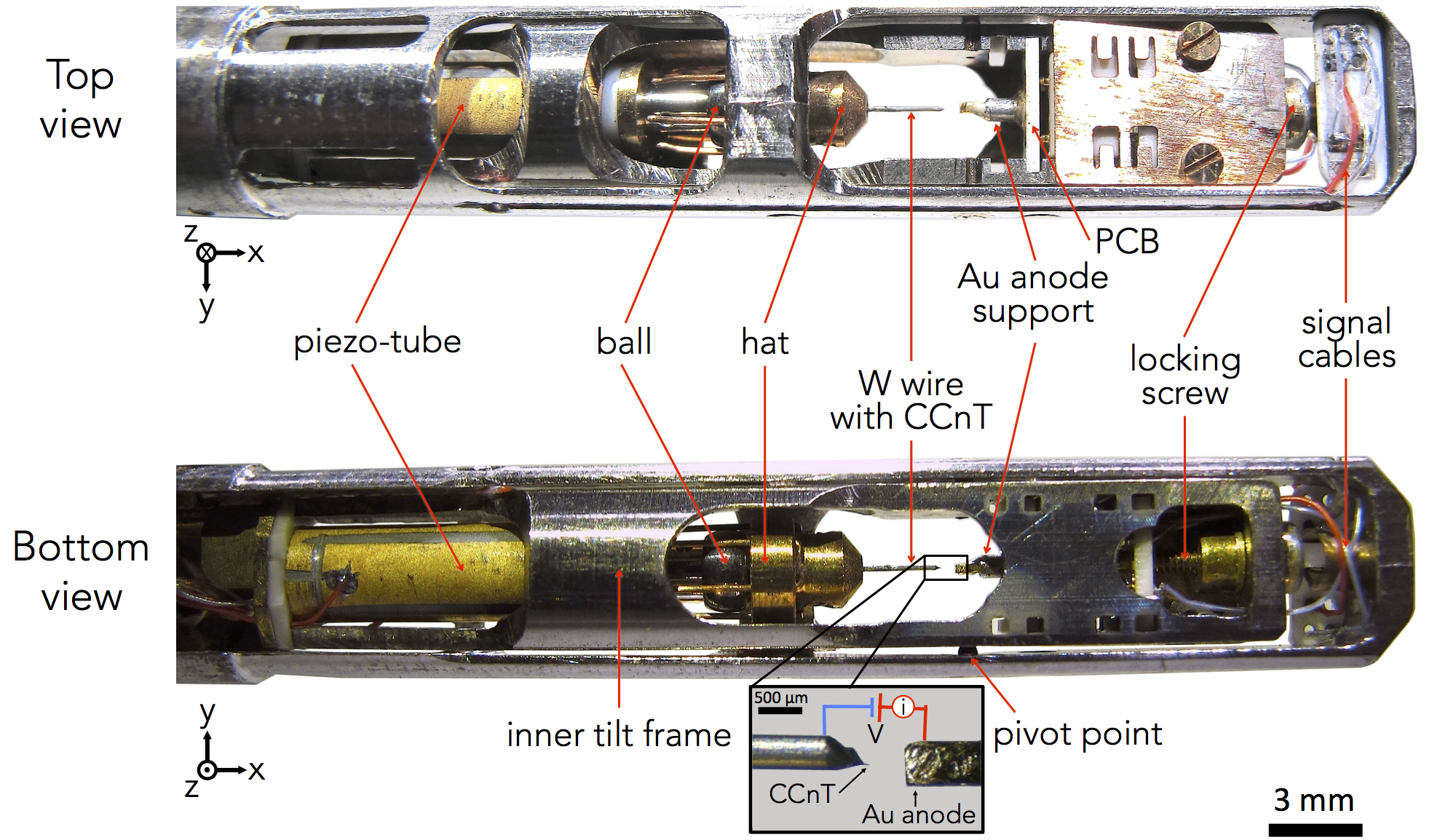
Fig. 1: The front part of the in situ TEM sample holder with a nanomanipulator for coarse and fine motion and biasing functionality. The inset shows the CCnT mounted on a wire in the nanomanipulator opposite the Au anode. |
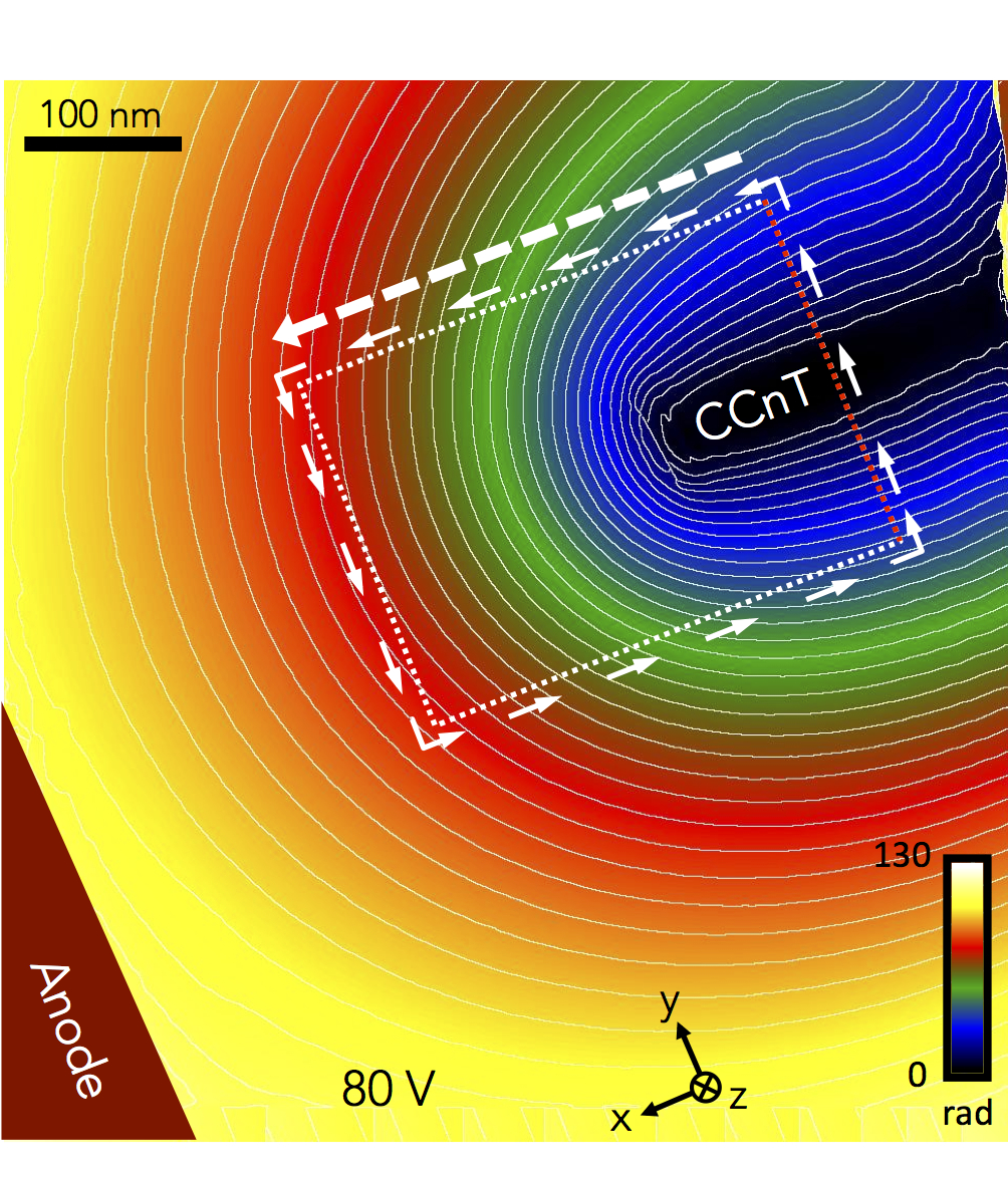
Fig. 2: Unwrapped hologram at field emission onset voltage of 80 V on the anode. The integration contour is indicated by small arrows, and the integration direction by the big, dotted arrow (analogous to the black dotted arrow in Fig. 3 a)). |
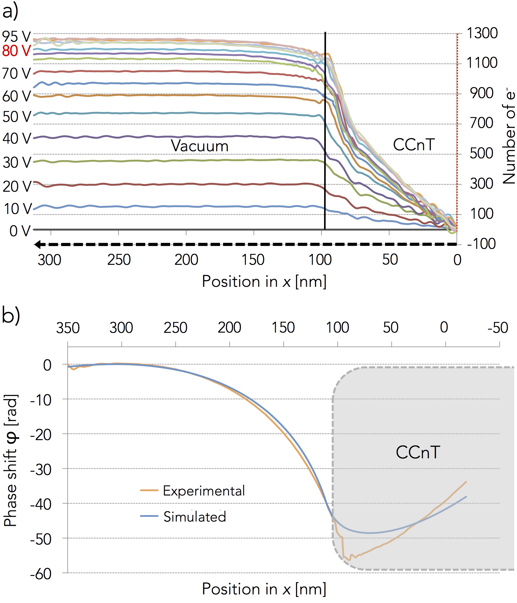
Fig. 3: a) Number of electrons along the CCnT and in the vacuum for different voltages. b) Profiles of phase shift maps from electron holography and finite element modeling. The bias on the anode was 80 V and the tip-anode separation distance 680 nm. |
|