IT-7-P-2779 In-situ TEM studies of the electromigration process in a single InAs nanowire
Electromigration (EM) is a phenomenon in which the electrical current flow of high density through a solid can lead to intensive atomic motion due to the high speed electrons transfer part of the momentum to the atoms (or ions) by collision. This phenomenon can lead to morphological and structural instabilities not only in metallic interconnections but also in semiconductor nanowires [1,2]. Since semiconductor nanowires are the subject of active study in virtue of their usage as low-dimensional systems, as building blocks for future nanoscale circuits [3], the EM becomes the key issue that controls the lifetime and stability of a nanoscale device.
In this work the process of EM in a single InAs nanowire was investigated by in situ TEM technique using a FEI Titan microscope operating at 300 keV. The EM experiments were carried out in a bias-ramping mode which allowed to perform accelerated experiments for EM process visualization in-situ TEM. The voltage applied for all cycles of EM experiments was set to 1200 mV. The resistivity calculated for the nanowire diameter 221 nm was 2*10-2Ω·cm. The current density for EM activation was about 3.6*104A/cm2. It was found that the EM in InAs nanowire starts at a position close to the cathode with formation of the cubic-shaped nanoparticles in the place of failure. The EDX analysis of the nanowire after EM experiments showed that the particle formed near anode part is indium. In the presentation all structural and chemical evaluations of the InAs nanowires during the electromigration will be discussed.
[1] D. Kang, T. Rim, C.-K. Baek, M. Meyyappan. Appl. Phys. Let. 103, 233504 (2013).
[2] C.-X. Zou, J. Xu, X.-Z. Zhang, X.-F. Song and D.-P. Yu. Journal of Appl. Phys. 105, 126102 (2009).
[3] Law, M., Goldberger, J., Yang, P. Annu. Rev. Mater. Res. 2004, 34, 83–122.
I would like to acknowledge ERC project 26792.
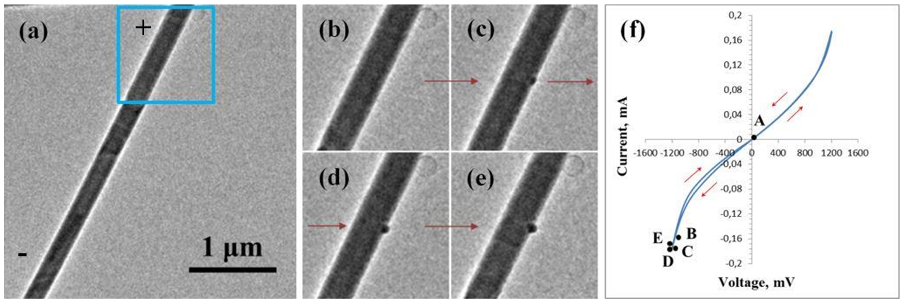
Fig. 1: Snapshots from the real-time TEM movie showing the first cycle of EM in InAs nanowire. (a) Initial configuration of InAs nanowire before EM experiments. (b)-(e) Images of the nanowire part pointed by blue square on (a) and taken at B- E times on I-V curve respectively. (f) Typical I–V curve. The red arrows indicate the bias-ramping direction. |
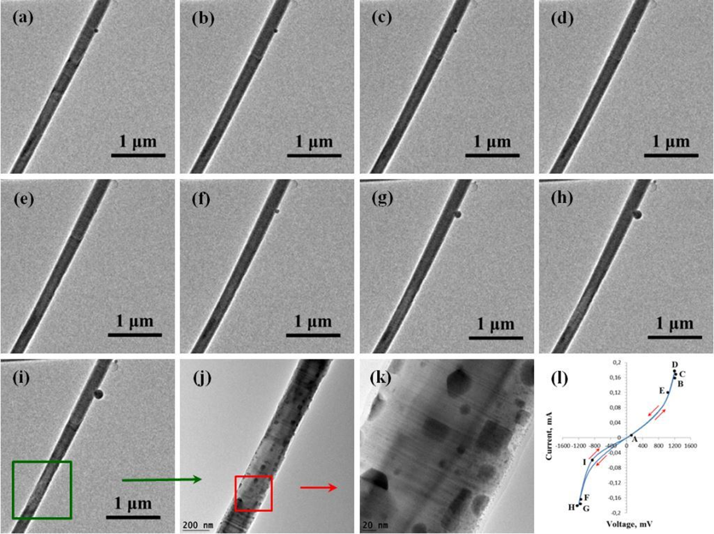
Fig. 2: Snapshots from the real-time TEM movie showing the 2nd EM cycle (a) Nanowire configuration after 1st EM cycle (b)-(i) TEM snapshots taken at B-I times on I-V curve respectively (j) TEM image of the nanowire part marked by green square on (i) (k) Magnified image of the nanowire part marked by red square on (j). (l) I–V curve for the 2nd EM cycle |