IT-9-P-2769 Automated crystal orientation mapping in TEM for the statistical analysis of microstructure evolution in nano-grained polycrystalline thin-films
Non-epitaxial polycrystalline films are important in many technological applications. Characterization of their microstructure is crucial for understanding their growth mechanisms and improving their properties. Their microstructure formation typically begins by dense nucleation of randomly oriented grains. During film thickening these grains impinge on each other, resulting in the overgrowth of unfavorably oriented grains and the subsequent formation of a textured film with a columnar or V-shaped grain structure. In this work our aim is to develop a methodology for quantitatively determining the grain size and orientation distributions throughout the thickness of such films, in order to help create accurate simulation models and to correlate film microstructures to their macroscopic properties.
The methodology is based on the principle of orientation mapping (OM); given the nm scale of the film microstructures, in this contribution we apply OM by nano-beam diffraction in TEM using a 2–3 nm electron probe and the NanoMEGAS ASTAR [1]. The high spatial resolution of this technique comes at the cost of needing suitably electron-transparent samples. A quantitative analysis of microstructure evolution requires the sample to have large thin areas from different heights within the film. These requirements can be met by a special double-wedge sample geometry previously proposed by Spiecker et al. [2], which provides continuous plan-view sections throughout the film thickness (see Fig. 1). The heights in the film of the plan-view sections are determined by cross-correlating the position of the thin area to the thickness of the film after dimpling, which was measured from visible light interferences after the dimpling step. Furthermore, the plan-view sections are perpendicular to the direction of the grain elongation thereby minimizing the regions of grain overlap within the projection of the specimen. This improves the reliability of the ASTAR measurements.
Here we report the application of this methodology to nano-grained polycrystalline low-pressure chemical vapor deposited ZnO films used as transparent conductive oxide layers in thin-film solar cells [3]. The applied methodology allows us to extract quantitative in-plane data on the evolution of grain size, orientation, and boundary misorientation as a function of height in the film (see Fig. 2), which can be compared to existing theory and simulations and help to provide new insights into the growth mechanisms that create these films.
References:
[1] EF Rauch et al., Microscopy and Analysis 22 (6) (2008) p. S5.
[2] E Spiecker et al., Acta Mater. 55 (2007) p. 3521.
[3] S Faÿ et al., Thin Solid Films 518 (2010) p. 2961.
The authors acknowledge funding from the SNSF, Grant Number 137833. L. Fanni, Dr S. Nicolay and Dr A. Hessler-Wyser of the IMT PV-lab, EPFL are thanked for the samples and discussions.

Fig. 1: Illustration of double wedge sample geometry. a) ZnO film on glass, b) dimpling of ZnO film (first wedge), c) wedge polish, d) bright-field TEM imaging at different heights along the electron transparent edge (red solid line) |
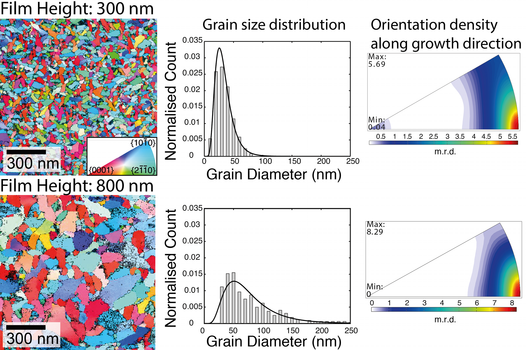
Fig. 2: Inverse pole figure maps overlaid with reliability index, extracted grain size and orientation distributions from two different heights in a ZnO thin film. The data demonstrate the ability of the methodology for obtaining quantitative data on nanocrystalline grain distributions along the height axis. |