IT-9-O-2763 Measuring strain with high precision and high spatial resolution using precession and convergent beam electron diffraction
Stimulated by the demand of the semiconductor industry, several new TEM based techniques have been recently proposed to measure strain with high sensitivity and high spatial resolution. In this presentation the interest of using diffraction techniques, either Convergent Beam Electron diffraction (CBED, fig. 1) or Nanobeam Precession Electron Diffraction (N_PED, Fig. 2 and 3) [1] will be shown. Off-axis CBED can give 3D maps of the complete 3D strain tensor ε or equivalently of the deformation gradient tensor F (Fig. 1b), but it is computationally and experimentally demanding. In constrast, N-PED is a straightforward and simple technique, although it is limited to the projected 2D strain tensor. Thanks to its robustness, great precision of about 2x10⁻⁴ and simplicity, N-PED should be the preferred tool for the microelectronics industry (Fig. 2).
Fig. 1 illustrates the principle of our strain measurement using off-axis CBED. The originality of our approach is to use both the deficient HOLZ lines of the transmitted beam and the excess HOLZ lines of the diffracted beams to measure the strain. Using Bloch wave calculated CBED patterns as tests, we could retrieve of 7 out of the 9 components of the deformation gradient tensor F (Fig. 1b); in particular the volume of the cells can be determined (Fig. 1c). By using two different directions which makes an angle of 22°, we show that it is possible to determines the whole tensor F. In addition, the method can also be extended to the analysis of split HOLZ lines that allow measuring the variations of the strain tensor along the electron beam.
For N-PED, best results were obtained on a FEI TITAN microscope using a 2kx2k CCD camera. Strain maps of 40x50 points can be acquired in about 20 minutes (Fig. 2). Precession can be used either with nearly parallel beam (NBED like condition, Fig. 3b) or with a convergent beam (on-axis CBED like condition, Fig. 3d). Slightly higher precision were obtained by using the CBED like condition. The main advantage of precession is to suppress the contrasts in the diffraction disks, which leads to improved strain precision.
A major advantage of diffraction based techniques is to be able to analyze samples of non-uniform thickness and non uniform composition along the electron beam. To demonstrate this, results on core shell nanowires (NWs) - Ge NWs embedded with SiN, or Si NWs with a surrounding polycrystalline gate - observed either parallel or perpendicular to the growth direction will be presented.
[1] J.L. Rouvière et al., Appl. Phys. Lett. 103 (2013) 241913.
This work was supported by several projects and contracts: the European catrene UTTERMOST project, the French ANR AMOS and the FEI-CEA common laboratory.
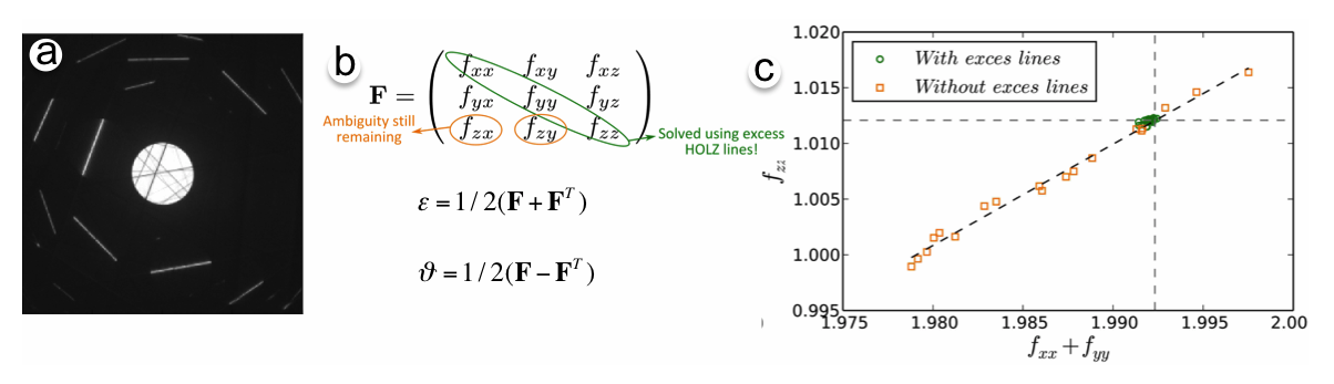
Fig. 1: (a) Simulated CBED pattern along a <651, 441,31> direction in Si. (b) Definition of the deformation gradient tensor F and its link to the strain tensor ε and rotation θ. (c) Without using the excess HOLZ lines, fzz and (fxx+fyy) are correlated. The volume (fzz+fxx+fyy) can be determined only by using the excess lines. |
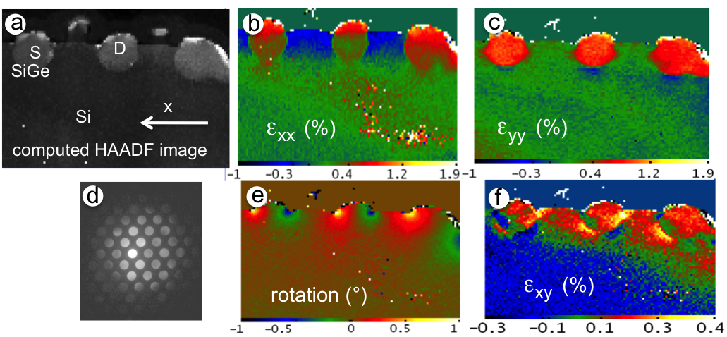
Fig. 2: Maps of 2 transistors with SiGe source (S) and drain (D). As SiGe has a greater lattice parameter than Si the Si channel is compressed by the SiGe source and drain in the x-direction (εxx). (a) HAADF image computed from the series of N-PED patterns. (b-c-e-f) Strain and rotation maps. d) A typical N-PED pattern of the series. |
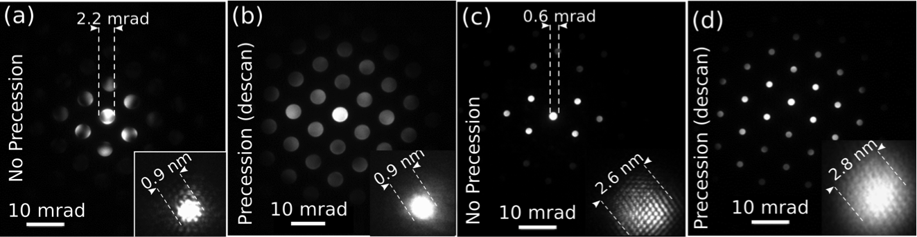
Fig. 3: Diffraction patterns obtained for various semi-convergence angles α and beam diameters d. At the bottom right of each diffraction, an image of the associated electron probe passing through the [011] silicon crystal gives an estimation of d. In (a) and (b) α = 0.6 mrad (NBED like condition), in (c) and (d) α = 2.2 mrad (CBED like condition). |
|