IT-5-O-2752 FIB-SEM Instrument with Integrated Raman Spectroscopy, Scanning Probe Microscopy and Secondary Ion Mass Spectroscopy
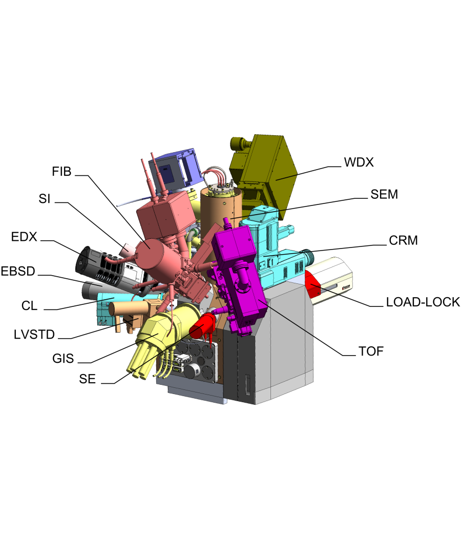
Integration of a number of techniques in a single tool gives the possibility of correlating multiple measurements and analyses of the same sample area, all made in-situ. A multifunctional tool comprising an SEM-FIB, an SPM and a TOF-SIMS has been presented recently [1]. Newly, a Confocal Raman Microscope (CRM) has been added to yield information about molecular composition and chemical bonds. The CRM image complements the high resolution SEM image, topographic image from SPM, chemical map from TOF-SIMS and sample modification by FIB. Fig. 1 shows the arrangement of the presented apparatus.
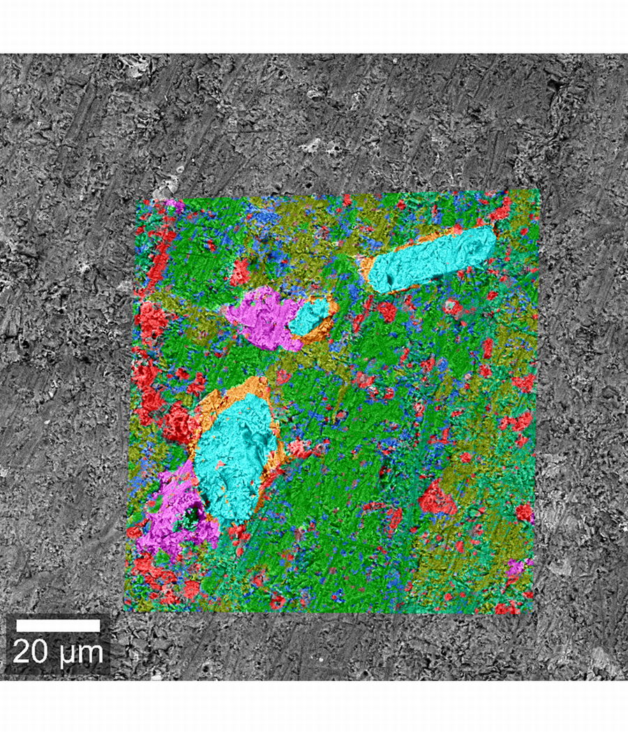
State-of-the-art Raman analyzers in SEMs use a parabolic mirror for focusing and lateral resolution is usually no better than 2-5 µm. The presented system provides a resolution of 360 nm by integrating a full confocal light microscope. The important property is the capability of Raman imaging. When a spectrum from a single point is acquired, one can never be sure if the position calibration is correct. Fig. 2 shows overlaid Raman and SEM micrographs of diorite sample. Besides lateral scanning, vertical movement is supported, which allows non-destructive 3D tomography.
Integration is possible with two alternative electron optical columns, each with a Schottky field-emission gun: the LYRA with a conventional objective lens or the GAIA with an immersion lens. The immersion lens column [2] is recommended for non-conductive or fragile samples, because it offers better resolution at low energies (1 nm at 15 kV and 1.4 nm at 1 kV).
The FIB is used to modify the sample and it also enables 3D tomography techniques by sequential FIB slicing followed by imaging to create 3D datasets with analytical information such as elemental composition, crystallographic information, etc.
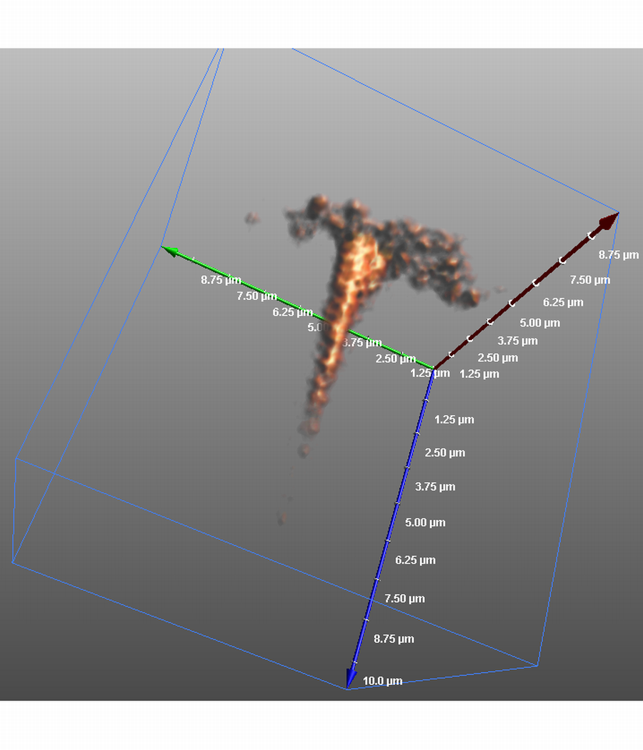
The FIB also acts as a primary ion beam for the TOF-SIMS analysis. It allows 2D as well as 3D spectral maps, carrying elemental, isotopic and chemical information about the investigated sample. Fig. 3 shows a TOF-SIMS 3D tomography of sodium contamination on solar cell sample. Lateral resolution of TOF-SIMS maps can be better than 50 nm.
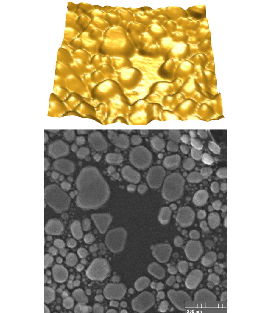
The integrated Scanning Probe Microscope (SPM) supports work in STM and AFM modes. Its compact design allows it to sit on the SEM stage. Simultaneous use of SPM, SEM and FIB enables a true depth calibration of TOF-SIMS depth profile as well as the calibration of 3D tomography techniques. The SPM head is designed for a depth resolution of 0.1 nm and an imaging speed of up to 20 s per image. Fig. 4 shows the AFM topography map of gold particles on carbon and corresponding SEM micrograph.
References:
[1] J Jiruše et al, Microsc. Microanal. 18 (Suppl. 2) (2012) p. 638.
[2] J Jiruše et al, Microsc. Microanal. 19 (Suppl. 2) (2013) p. 1302.
The research leading to these results has received funding from the European Union Seventh Framework Program [FP7/2007-2013] under grant agreement No. 280566, project UnivSEM.


