IT-11-P-2738 Nanoscale strain analysis by dark-field electron holography of shallow trench isolation structures for MOSFET technology
As microelectronic devices shrink, mechanical deformations induced by the various fabrication process steps play a growing role in their technological properties. These parameters must be understood and controlled because strained silicon can significantly boost transistor performance [1], but can also lead to product failures. Of interest in this study are transistors based on shallow trench isolation (STI) structures (Fig 1.) used in metal-oxide-semiconductor field effect transistor (MOSFET) technology. The main goal is to understand the mechanisms responsible for strain formation inside the active silicon area.
Off-axis dark field electron holography (DFEH) in TEM is used to perform the strain analysis on dedicated test structures that simulate the mechanical deformation on the active silicon areas that are supposed to receive the MOSFET. The choice of removing the MOSFET was made in order to analyze/evaluate purely the influence of the STI structure, within a systematic study of the influence of STI fabrication steps. The DFEH technique [2] is based on the interference of diffracted beams coming from two different regions of the sample with the aid of an electrostatic biprism (Fig. 2). If the two regions present a lattice constant difference, a phase difference will be measured from the holographic fringes and the strain information can be retrieved.
For the experiments, classical focused ion beam (FIB) TEM lamellae were prepared but thickness variations due to the STI geometry and lamella bending due to strain relaxation prevented the extraction of the strain tensor from the entire structure. For this reason, a dedicated sample preparation method has been developed to match the requirements imposed by the DFEH method (i.e. uniform 120 nm sample thickness with no specimen bending). Backside FIB milling [3] combined with an innovative “double-bar” rigid-thin TEM lamella geometry succeeds in avoiding these artefacts (Fig. 3). Measurements made on the HITACHI I2TEM at CEMES-CNRS (Toulouse, France) now permit the extraction of the complete sample-plane strain tensor in the active silicon area sandwiched by two STI structures (Fig. 4). The results are in accordance with values obtained by CBED and TCAD simulations in the literature [4].
[1] M. Cai et al., IEEE Trans. Electron Devices, vol. 57 (2010) 1706–1709
[2] M. Hÿtch et al., Nature, vol. 453 (2008) 1086–1089.
[3] J. Gazda et al., Microsc. Microanal., vol. 16 Supplement S2 (2010) 230–231.
[4] A. Steegen and K. Maex, Mater. Sci. Eng. R Rep., vol. 38 (2002) 1–53.
The authors acknowledge funding by the Swiss Commission for Technology and Innovation (CTI), Franc Fort project number 13496.1 PFFLE-NM, and ESTEEM2 for Transnational Access to the I2TEM at CEMES. Marco Cantoni at CIME is thanked for many useful discussions.
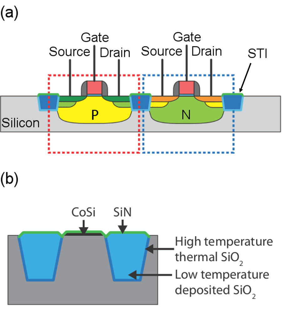
Fig. 1: Schematic figures of CMOS transistor (a) and STI structures (b). |
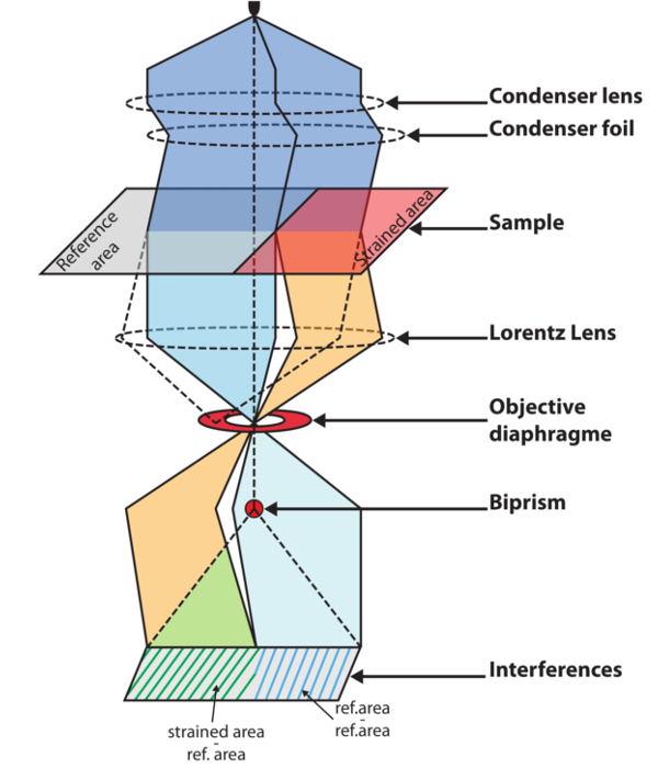
Fig. 2: Principle of the dark-field electron holography (DFEH) technique. |
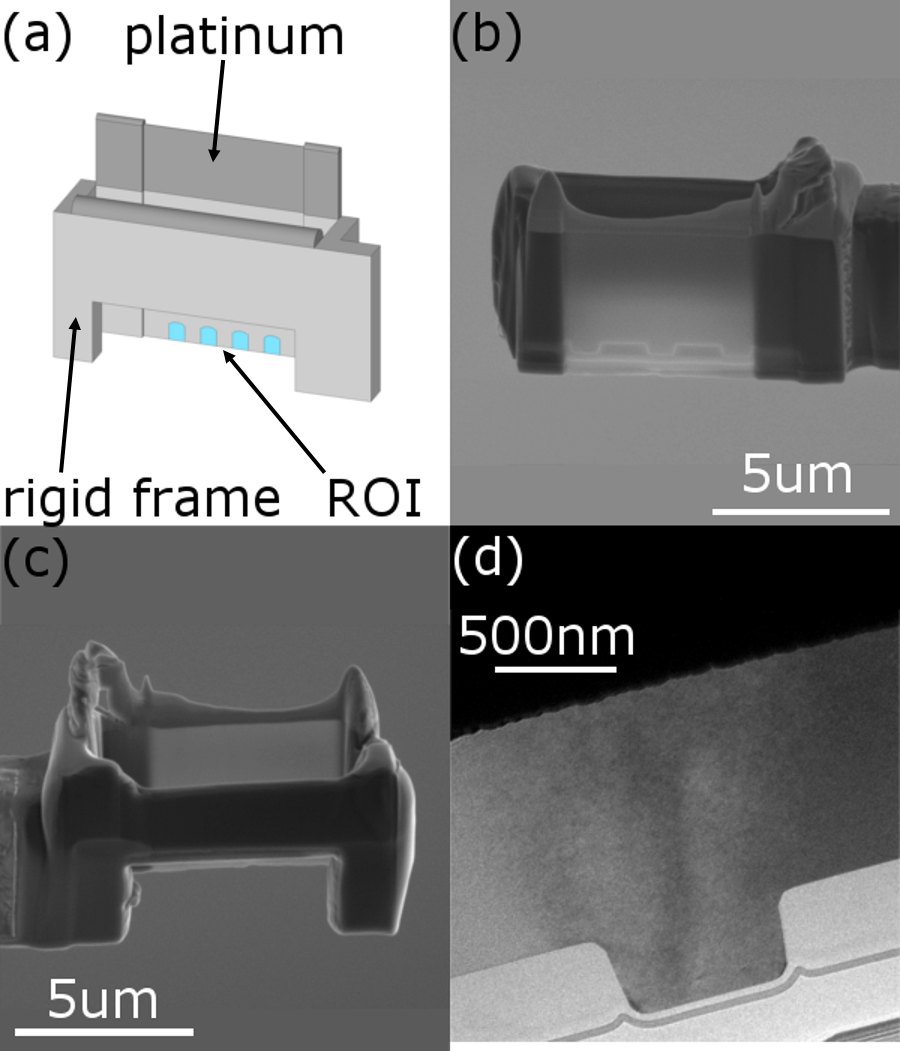
Fig. 3: The double-bar “rigid-thin” TEM lamella geometry (a). SEM images of the thin part (b) and the rigid frame (c). Bright-field TEM image of the region of interest (d). |
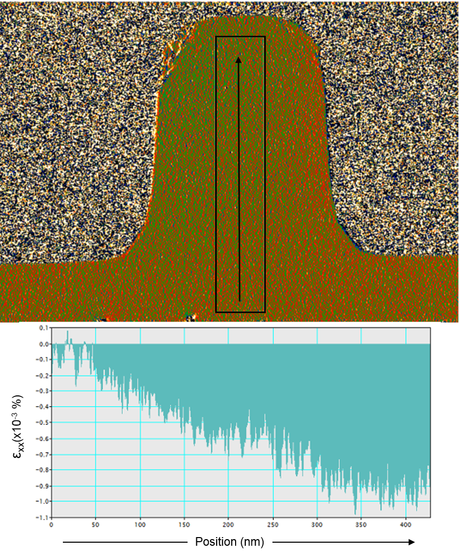
Fig. 4: Strain measurement of the active silicon area sandwiched by STIs. |