IT-11-P-2718 80 kV double biprism electron holography
Off-axis electron holography is a powerful method to retrieve the image phase in high quality[1]. Recently, off-axis electron holography performed with an acceleration voltage of 80 kV has moved into the focus of interest because electrons accelerated with 80 kV produce less knock-on damage and hence can be used to investigate, e.g., carbon-based materials [2]. The performance of a double biprism setup at 80 kV acceleration voltage and possible advantages in comparison to 300 kV were investigated.
A FEI Titan transmission electron microscope equipped with a high-brightness Schottky field-emission gun, an image Cs-corrector and a 2k by 2k camera (Gatan US1000) was used for this work. The camera's modulation transfer function (MTF) was determined with the edge method (fig. 1). The MTF is significantly improved at an acceleration voltage of 80 kV compared to 300 kV, probably due to a smaller electron scattering volume in the scintillator. The improvement is best for a sampling rate of about 10 pixels per fringe, giving an improvement factor of 1.9. In experimental electron hologram series with different fringe spacings, but keeping a sampling rate of 10 pixels per fringe realized by accordingly adjusting the magnification, about the same improvement of the standard deviation of the reconstructed phase was measured (fig. 2). Thereby, other effects like, e.g., electron energy dependent detection quantum efficiency of the camera, seem to be negligible.
To further decrease the standard deviation of the reconstructed phase and hence improve the phase sensitivity, a double biprism setup [3] was used. It allows the minimization of the applied biprism voltages. With the resulting increased stability of the holographic system, longer exposure times are possible, leading to an observed standard deviation of the reconstructed phase of about 2π/740 in a single empty hologram with an exposure time of 20 s.
The 80 kV off-axis electron holography is demonstrated using a thin GaN-foil oriented along [11-20] zone axis. Here, to avoid image resolution due to specimen drift, ten holograms with an exposure time of two seconds were made and averaged. The residual lens aberrations in the reconstructed image wave were corrected to retrieve the object exit wave. For comparison with the experiment, a GaN foil with thickness 1.9 nm, a chromatic aberration of 1.3 mm and an energy spread of 0.8 eV was simulated (fig. 3) [4]. Amplitude and phase of the object exit wave show a good match to the simulation.
- M. Lehmann et al., Microscopy and Microanalysis 8 (2002), p. 447-466.
- M. Linck et al., Microscopy and Microanalysis 18 (Suppl 2) (2012), p. 478.
- K. Harada et al., Applied Physics Letters 84 (2004), p. 3229.
- P. A. Stadelmann, Ultramicroscopy 21 (1987), 131.
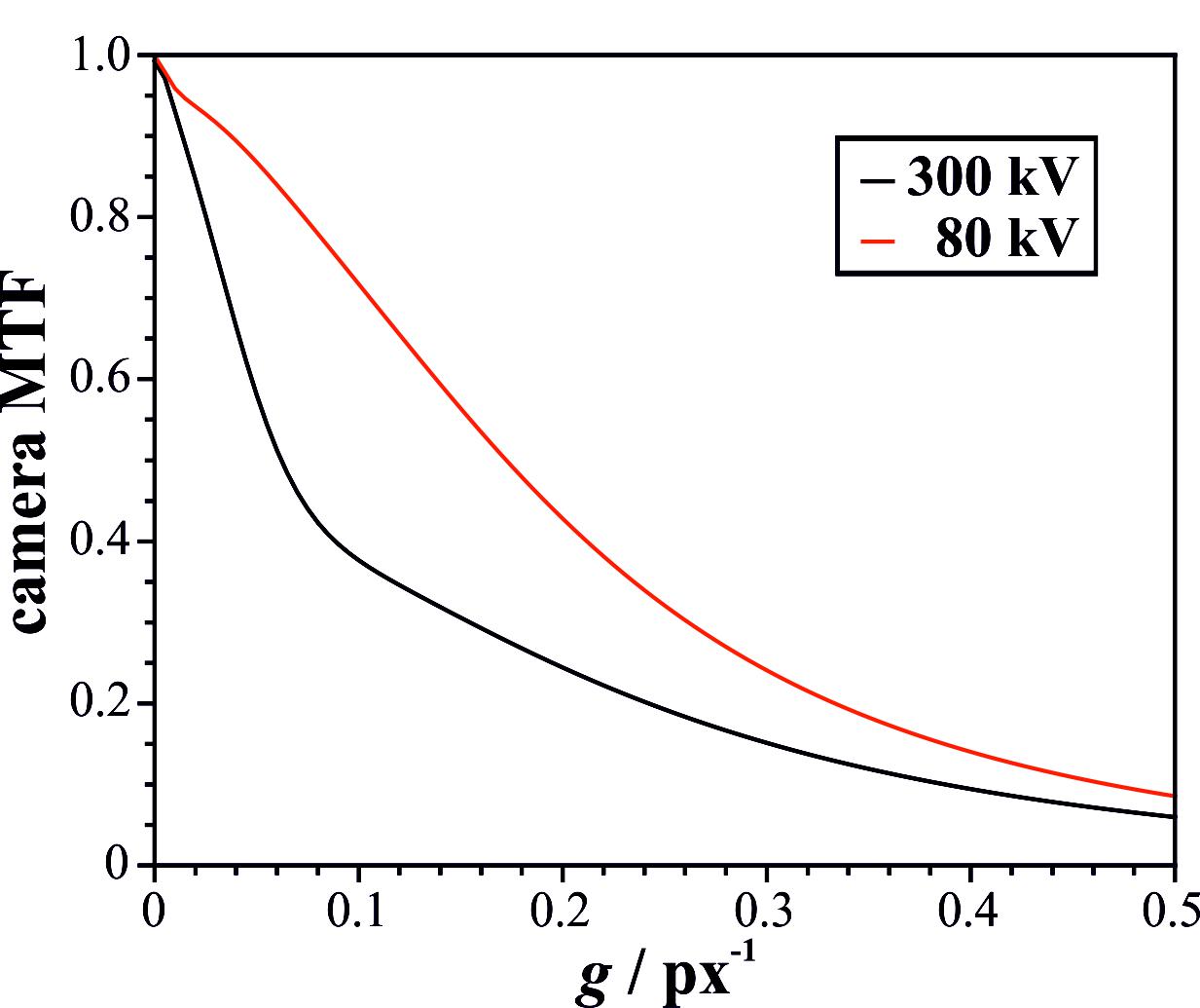
Fig. 1: Damping by the modulation transfer function (MTF) of the camera as a function of the sampling frequency g at acceleration voltages of 80 kV and 300 kV. |
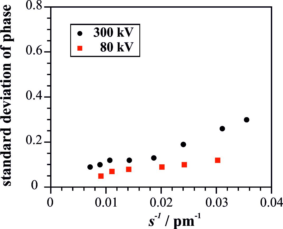
Fig. 2: Standard deviation in the reconstructed phase of electron holograms with a sampling rate of 10 pixels per hologram fringe as a function of the inverse fringe spacing s related to the object plane. The exposure time was 2 s. A smaller standard deviation is equivalent to a higher phase sensitivity. |
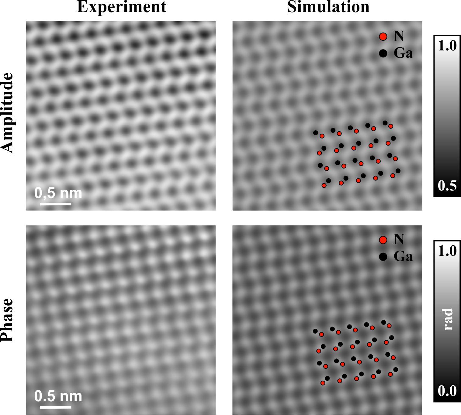
Fig. 3: Comparison of experimental and simulated object exit-wave of a thin GaN foil in [11-20]-orientation with a thickness of approximately 1.9 nm. Both amplitude and both phase images have the same grey levels. |
|