IT-13-IN-2711 Advances in FIB Nanotomography
FIB-tomography is used in materials science for 3D-analysis of nanostructured materials [1]and in life science for the analysis of complex structures like brain tissue [2]. This presentation summarizes recent technological improvements, which include advancements in detector technology for electron imaging and elemental analysis, scan generator technology for high throughput imaging, and automated drift correction for reliable 3D reconstruction. New in-column detectors have a higher sensitivity for low energy electrons, which is the basis for a very high resolution down to a few nm voxel size. The low kV imaging can be combined with energy filtering in order to detect a pure signal of backscattered electrons (BSE), which improves the reliability of phase segmentation and quantitative analysis. The quality of the 3D reconstructions can also be improved with refined procedures for drift correction based on reference marks. In addition, with the new scan generators image acquisition and ion milling can be performed synchronously. In this way the acquisition speed increases further. Finally, spectral and elemental mapping (XEDS) based on Silicon Drift Detectors (SDD) provides higher X-ray count rates. Increased acquisition rates open new possibilities in chemical analysis that provide larger data cubes with higher representativeness. The new possibilities of FIB-tomography are illustrated with the following examples: a) Reliable phase segmentation is discussed for a superconducting material with trapped pores that cannot be filled with resin. b) Combined analysis of SE- and BSE stacks reveals the complex microstructure of a Sn-solder with different nano-sized precipitates [3] and c) High throughput elemental analysis is performed of a NiTi stainless steel with a complicated multi-phase microstructure [4]. The examples document the recent advancements in resolution, contrast, stability and throughput, which are necessary for reliable and representative 3D-analysis.
References
1. L. Holzer, M. Cantoni, in Nanofabrication Using Focused Ion and Electron Beams—Principles and Applications, I. Utke, S. Moshkalev, P. Russell, Eds. (Oxford University Press, New York, 2012), pp. 410–435.
2. M. Cantoni, C. Genoud, C. Hébert and Graham Knott, Microsc. & Anal. 24(4): 13-16 (2010)2010.
3. M. Maleki, J. Cugnoni, J. Botsis, Acta Mater. 61 (1), (2013).
4. P. Burdet, J. Vannod, A. Hessler-Wyser, M. Rappaz, M. Cantoni, Acta Mater. 61 (8), 3090 (2013).
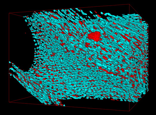
Fig. 1: Fig 1. Three-dimensional representation of the two different intermetallic phases in the SnCuAg-type solder, segmented based on simultaneously acquired secondary electron and backscattered electron image stacks. |
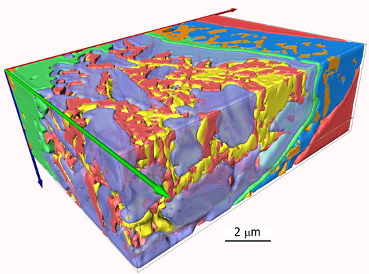
Fig. 2: Fig 2. Complex chemical microstructure of a NiTi—stainless-steel weld with different phases. The yellow and red phases are chemically very close and required segmentation based on the secondary electron image contrast. |