IT-13-P-2701 High performance nanomachining using the new analytical FIB-SEM system
A new analytical tool GAIA, combining high performance Focused Ion Beam (FIB) column with ultra-high resolution Scanning Electron Microscope (SEM), has been developed. The SEM resolution has been improved down to 1 nm at 15 kV and 1.4 nm at 1 kV, see Figure 1, thanks to a new objective lens of a single-pole immersion type [1, 2]. It creates a strong magnetic field surrounding the sample and decreasing optical aberrations. Intermediate lens enables to work in the magnetic-field-free mode suitable for analysis, magnetic sample imaging and observation during FIB machining. FIB milling process can be controlled by SEM imaging simultaneously, because of two independent scanning generators and sophisticated TESCAN detection system. Besides chamber detectors for detection of secondary (SE), backscattered (BE), transmitted (TE) electrons and secondary ions (SI), InBeam SE and InBeam BE detectors placed in the column give the free space around the sample.
The new non-magnetic Cobra FIB column with high resolution of 2.5 nm at 30 kV [3] and great performance at high currents has been designed to protect from the influence on the magnetic field of the immersion SEM objective lens. DrawBeam software allows drawing of patterns in CAD-like GUI for electron and ion beam lithography. The patterns are generated by ultra-fast scanning generator with pixel dwell time down to 20 ns. The novel milling strategy is included in DrawBeam software for 2.5 times faster FIB cross sectioning, see Figure 2. The technique is based on the correction of the intended shape to maximize the milling rate and to minimize the redeposition effects. The new AutoSlicer software for the automated cross sectioning and TEM lamella preparation increases FIB performance even further, see Figure 3. FIB column control is greatly simplified by using TESCAN In-Flight Beam TracingTM technology, which newly enables to compute and optimize FIB column settings.
GAIA instrument is prepared for fabrication and observation of non-conductive samples. Charge accumulation on the surface caused by FIB milling can be neutralized by integrated electron flood gun or SEM electron beam. SEM imaging without charging artifacts can be performed at critical energy, below 4 keV, with improved resolution. TESCAN beam deceleration technology, applying negative voltage on the sample, allows automatic control of the electron landing energy down to 50 eV (manually down to 0 eV) and it further improves SEM resolution at low beam energies, see Figure 1. The new control module provides sample discharge and touch-alarm protections.
References:
[1] Z Shao et al, Rev. Sci. Instrum. 60 (1989) p. 3434.
[2] J Jiruše et al, Microsc. Microanal. 19 (Suppl 2) (2013) p. 1302.
[3] A Delobbe et al, EFUG 2011, http://www.imec.be/efug
The research leading to these results has received funding from the European Union Seventh Framework Program [FP7/2007-2013] under grant agreement No. 280566, project UnivSEM.
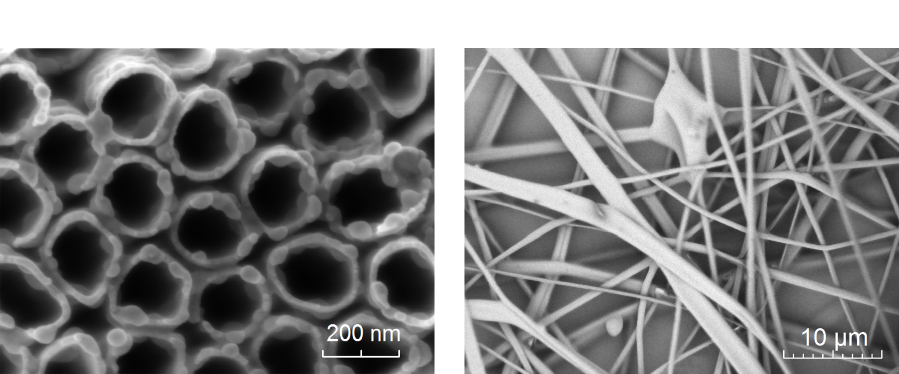
Fig. 1: Ultra-high resolution at low beam energies: TiO2 nanotubes at 1 kV (left) and polymer nanofibers at 20 V (right). |
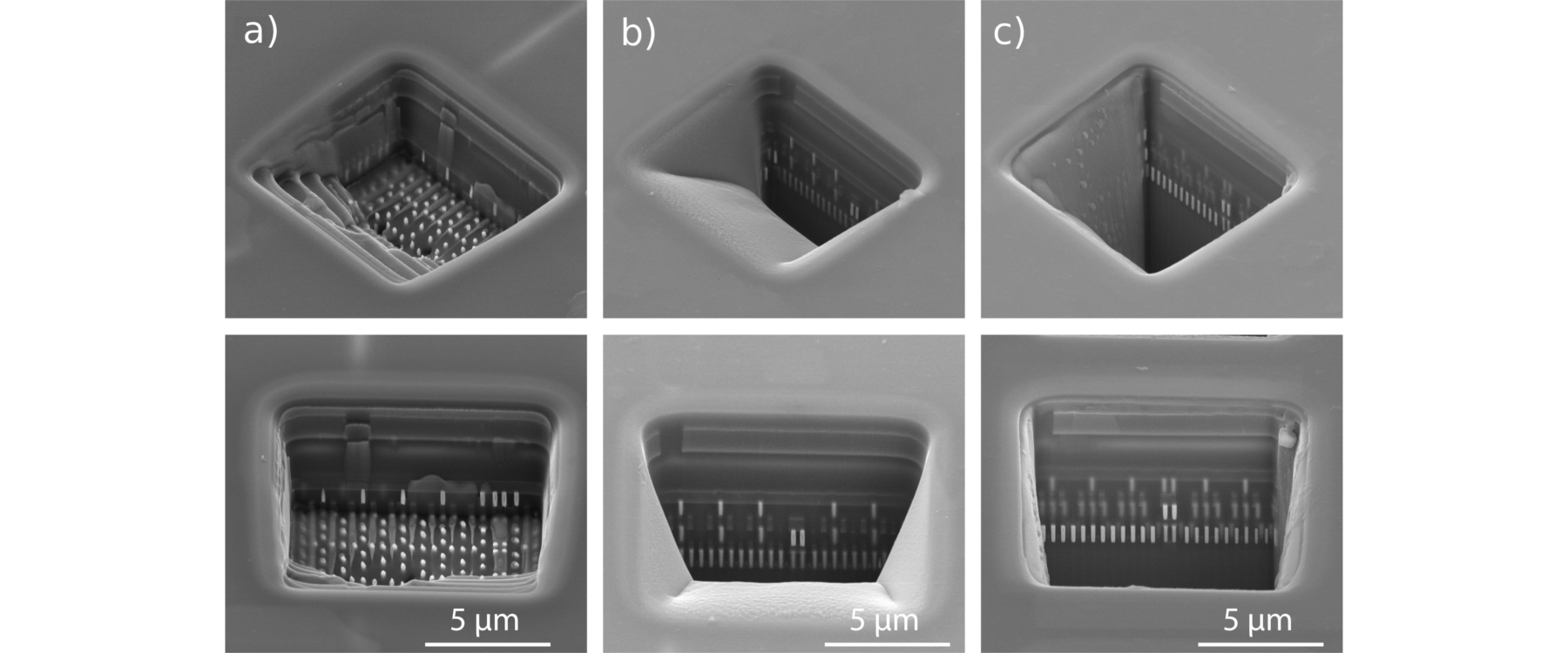
Fig. 2: Different approaches for cross section preparation: (a) basic top-down “staircase” strategy, (b) a single-pass cross sectioning with high redeposition, (c) a fully optimized cross section object with 2.5 times higher milling speed, the highest depth and the best shape without redeposition. Milled using 12 nA FIB current at 30 keV. |
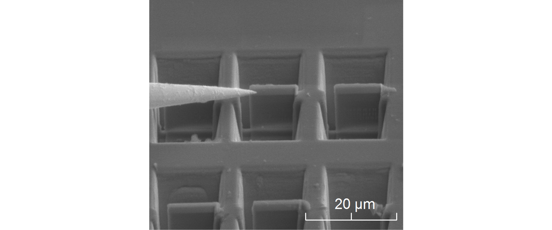
Fig. 3: Automated TEM lamella preparation utilizing innovative fast cross section milling approach. |
|