IT-2-O-2674 Fast imaging with inelastically scattered electrons by off-axis chromatic confocal electron microscopy
Imaging with inelastically scattered electrons is an important method for studying the composition and electronic properties of materials down to the atomic scale [1]. In this work, we describe an approach for fast mapping of inelastically scattered electrons using a scanning transmission electron microscope in a confocal mode, without using a spectrometer. We develop an off-axis scanning confocal electron microscope configuration using a double spherical-aberration corrected STEM/TEM. The electron probe is focused onto the sample at a significant angle to the optic axis of the imaging lens (Fig 1) and the probe-corrector retuned to form an atomic-scale electron probe in the specimen plane. Under the effect of the chromatic aberration of the imaging lens system, electrons with a chosen energy loss, the confocal energy, Ec, can be focused to a confocal point on the detector plane, while electrons of all other energies, including the zero loss electrons, will be chromatically defocused at that plane. In addition, the tilting of the incident beam laterally shifts the object exit wave in the back focal plane of the imaging lens, introducing an energy-related lateral displacement of the defocused probe. The inelastically scattered electrons are then chromatically dispersed both parallel and perpendicular to the optic axis, effectively separating electrons with different energies. In particular, electrons with the confocal energy can be detected selectively using an integrating detector. Using a synchronized set of scan-descan coils, these confocal electrons can remain focused on the detector as the electron probe is scanned across the specimen (Fig 1).
We illustrate the method with nanoscale core-loss chemical mapping of silver (M4,5) in an aluminium-silver alloy and atomic scale imaging of the low intensity core-loss La (M4,5@ 840eV) signal in LaB6 (Fig 2). The scan rates are up to 2 orders of magnitude faster than conventional STEM spectrum imaging methods recorded by CCD, enabling a corresponding reduction in radiation dose and improvement in the field of view [2]. Moreover, this off-axis chromatic confocal configuration offers the potential for fast nanoscale three-dimensional chemical mapping when coupled with the improved depth and lateral resolution of the incoherent confocal mode [3].
[1] R. F. Egerton, Electron energy-loss spectroscopy in the electron microscope (Plenum Press, New York, 1996), 2nd edn.
[2] C. Zheng, Y. Zhu, S. Lazar, J. Etheridge, Physical review letters, accepted (2014).
[3] T. Wilson and C. Sheppard, Theory and practice of scanning optical microscopy (Academic Press, London ; Orlando, 1984)
Funding is acknowledged from the Australian Research Council Grants DP110104734 and LE0454166.
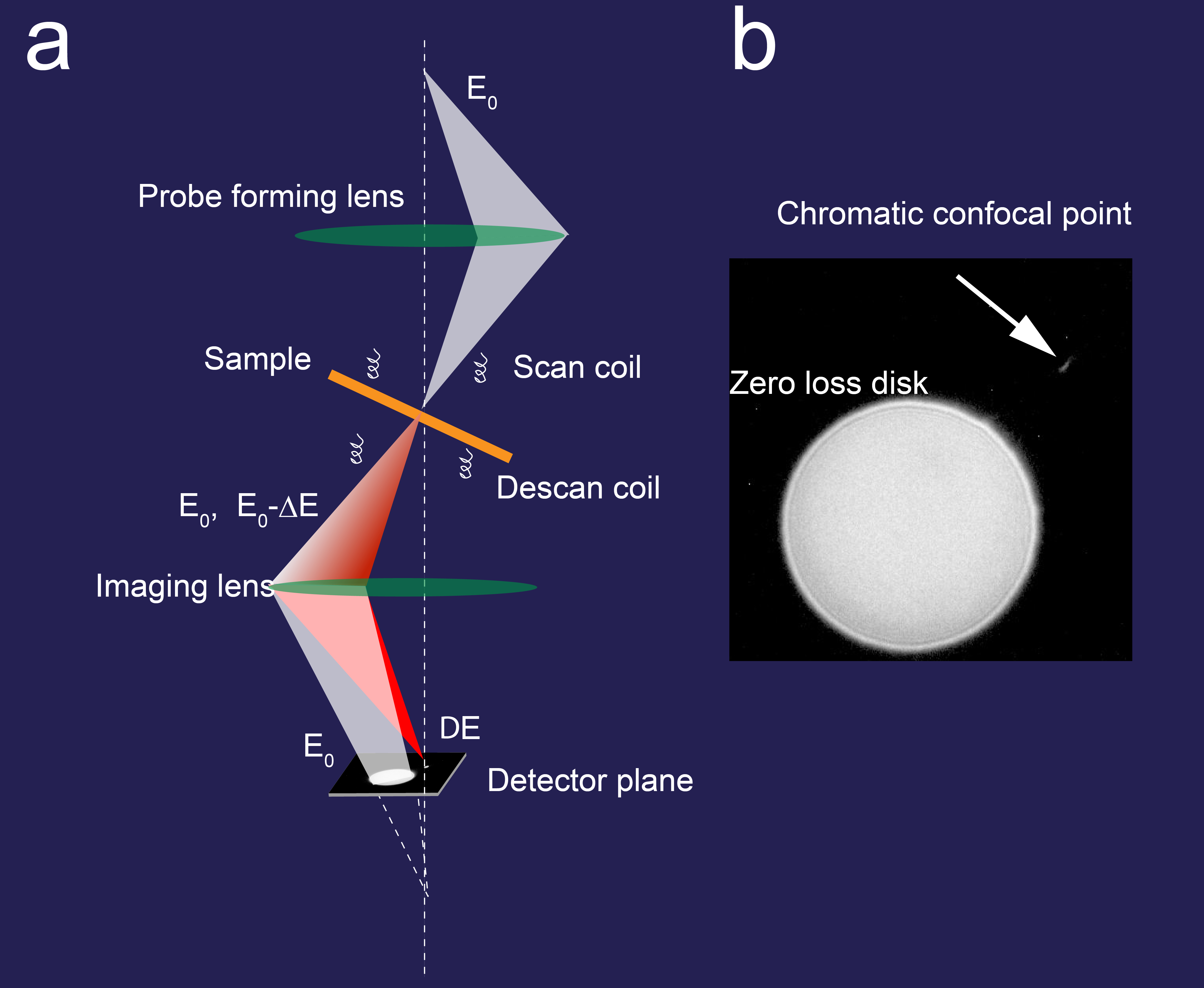
Fig. 1: (a) Optical diagram of off-axis scanning confocal electron microscopy. (b) Chromatic defocused probe image of amorphous carbon. The refocused chromatic confocal energy is centered at energy loss of 300 eV. Chromatic confocal point is indicated by the arrow. |
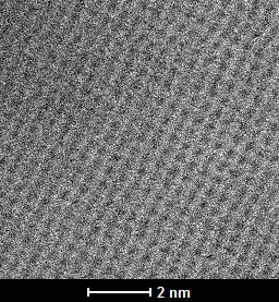
Fig. 2: Atomic resolution off-axis SCEM map of lanthanum M4,5 (~840 eV) core loss electrons in LaB6. The pixel dwell time is 1.5 ms with image size 256 x 256. |