IT-5-P-2665 Electron energy-loss mapping of a perovskite-based solar cell
The investigation of nanomaterials for solar cells, aimed at determining chemical structure and morphology, is a vital step in the development of novel materials to face the current energy crisis. Thin film solar cells have been evolving in the last decades, attaining interesting performance levels. In particular, highly efficient perovskite-based solar cells were demonstrated last year [Liu2013], and there is booming interest in the design of such systems. The addition of metal-oxide core-shell nanoparticles is also being investigated in several thin film devices for increasing light harvesting.
Morphology, both at the nano- and the micro-scale, plays a major role in several processes which affect the behaviour of thin film solar cells. Focused Ion Beam milling (FIB) processing is a powerful tool to extract samples from a full solar cell device for analysis with a transmission electron microscope (TEM). Characterisation in a TEM can shed light on the local elemental composition of the device, as well as spatially-resolved information on the electronic energy levels.
Recent developments in TEM analytical capabilities have enhanced the possibilities for investigation further: brighter electron guns and new detectors for energy-dispersed x-ray spectroscopy (EDX) and electron energy-loss spectroscopy (EELS) now allow large spectrum images to be acquired quickly. As a consequence, devices with organic components can be examined with a reduced electron irradiation, limiting beam damage artifacts.
In this work we apply FIB preparation to a perovskite-based solar cell and investigate the morphology of the photoanode using TEM. Elemental and EELS maps are acquired, and the effect of plasmonic nanoparticles is investigated. Information on the spatial distribution of metal nanoparticles is extracted to provide feedback on the device fabrication process.
Spectrum images are analysed using principal component analysis and blind source separation to optimise signal-to-noise ratio, thus obtaining high quality maps while limiting the electron dose on the specimen. This procedure also naturally separates different compounds without introducing operator bias, and is particularly effective in the presence of complex compounds, such as the perovskite active layer.
[Liu2013] M. Liu, M. B. Johnston and H. J. Snaith, Nature 501, 395–398, 2013
GD, XP, FDLP and CD thank ERC for funding.
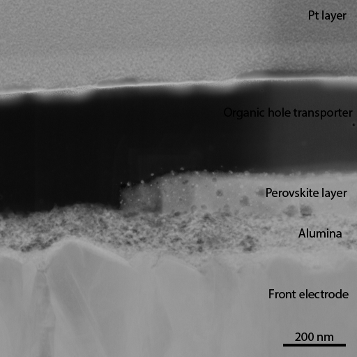
Fig. 1: Cross-sectional view of a perovskite-based solar cell. |