IT-2-O-2658 Atomic resolution secondary electron imaging and simulation of the SrTiO3 (001) c(6x2) surface reconstruction
Aberration-corrected scanning transmission electron microscopes (STEM) enable simultaneous collection of atomically resolved signals relating to coherent scattering (bright field and annular bright field imaging), structural information based on thermal scattering to large angles known as high-angle annular dark-field (HAADF) imaging, bonding information using electron energy-loss spectroscopy (EELS), and element identification using both EELS and energy dispersive x-ray spectroscopy. Atomic resolution imaging based on secondary electron (SE) signals was demonstrated in 2009 [1], but the technique is only slowly growing in use. While these SE signals are highly surface sensitive due to the narrow escape depth of electrons with energies <50eV [2], atomic resolution SE imaging of surface structures that differ from a simple bulk crystal termination has not been previously demonstrated.
We have recently imaged the c(6×2) reconstruction on the (100) surface of single crystal SrTiO3 (Fig 1) through simultaneous atomic resolution SE and HAADF STEM with complementary HREM imaging. The ability to simultaneously record surface sensitive SE and bulk dominated HAADF signals at atomic resolution makes the problem of surface structure registration to the bulk lattice highly tractable, which is a distinct advantage over other scanning probe methods. By inspection it is clear that the registration of the previously reported structure, primarily refined from surface x-ray diffraction and scanning tunneling microscopy (STM) experiments [3], is incorrect. Interpretation of the experimental SE measurements from first principles is now possible using a recently developed quantum mechanical model to simulate SE images. This approach takes into account the probability and angular distribution of electrons that are ejected from atoms in the specimen when ionization of both core and semi-core electrons occurs [4]. Our preliminary simulations of a newly proposed structure of the SrTiO3-<100>-c(6×2) reconstruction are in good agreement with the bulk-subtracted experimental SE data (Fig 2), and consistent with previously reported data from STM, Auger spectroscopy, and x-ray diffraction measurements. The structure solved by SE imaging is also stable in density functional theory simulations, and is on the thermodynamic convex hull of known reconstructions on SrTiO3 <100>.
[1] Y Zhu et al., Nat. Mater. 8 (2009) p. 808
[2] A Howie, J. Microsc. 180 (1995) p.192
[3] CH Lanier, et al., Phys. Rev. B 76 (2007) 045421
[4] HG Brown et al., Phys. Rev. B 87 (2013) 054102
A portion of this work was performed at NCEM, supported by the Office of Science, Basic Energy Sciences of the U.S. Department of Energy under Contract No.: DE-AC02-05CH11231.
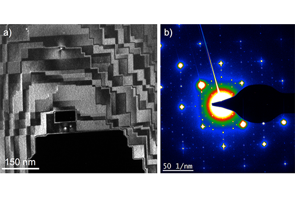
Fig. 1: (a) Weak beam dark field image of SrTiO3 001 c(6x2) single crystal with g=(200) showing atomically flat terraces (b) Transmission electron diffraction pattern of the c(6x2) reconstruction with c2mm symmetry acquired off-zone to minimize bulk dynamical diffraction |
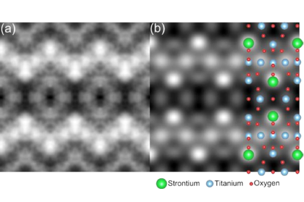
Fig. 2: (a) Bulk subtracted experimental secondary electron image of a 6×2 unit cell surface reconstruction on a <100> SrTiO3 substrate averaged over ~600 unit cells with c2mm symmetry enforced. The 200-keV probe had a convergence semi-angle of 25 mrad. (b) Prelimenary simulation of the result in (a) using the (projected) surface reconstruction indicated. |