IT-2-O-2644 Low-voltage and energy-filtered chromatic aberration-corrected high-resolution TEM on the PICO instrument
The advent of chromatic aberration correction in the transmission electron microscope (TEM) offers new prospects for high-resolution imaging at low accelerating voltages and for energy-filtered TEM (EFTEM). Examples of low voltage and energy-filtered images of complex oxides, thin layered materials, and nanoparticles will be presented, demonstrating the unique optical properties of an achroplanatic CEOS CCOR Cc/Cs corrector on Jülich’s chromatic aberration-corrected “PICO” microscope.
Atomic-resolution imaging at low voltages, currently down to 50 kV, allows high-resolution studies of radiation-damage-sensitive nanomaterials, such as CdSe/CdS nanostructures obtained from a cation exchange reaction, graphene and carbon nanotubes. It is also beneficial for the study of organic ligands, ligand-stabilised materials and materials that are functionalized with organo-metallic compounds.
The ability to acquire dose-efficient atomic-scale EFTEM elemental maps using the achroplanatic CCOR corrector on this microscope with a large field of view and large energy windows results from the fact that the chromatic focus spread is negligible after chromatic aberration correction. Figure 1 shows an example of an atomic-resolution elemental map of Ca obtained from a thin TEM foil of a calcium-titanate/strontium-titanate multilayer. Figure 2 shows a structural and compositional modulation in a (CeS)1.2CrS2 misfit-compound nanotube, which comprises alternating hexagonal CrS2 and rock-salt CeS sheets that have a repeat period of 11.2 Ångstrom.
The quantification of EFTEM elemental maps to provide atomic-resolution information about the local chemical composition of a specimen is complicated by the preservation of elastic contrast due to elastic scattering, which gives rise to thickness and defocus dependent contrast with fine details at all energy losses. Optical stability over minutes of collection time and careful image alignment and background subtraction are also required to obtain meaningful and reliable atomic-scale EFTEM elemental maps.
The authors thank J. Schubert (Forschungszentrum Jülich) and L. Penchakarla and R.Tenne (Weizmann Institute of Science) and M. Bar Sadan (Ben Gurion University) for kindly providing the materials used in this study
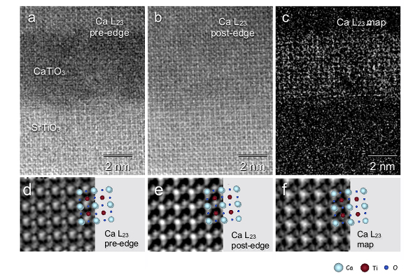
Fig. 1: High-resolution EFTEM images of a CaTiO3/SrTiO3 [001] multilayer sample taken at 300 kV. Ca L23 (a) pre-edge image, (b) post-edge image and (c) background-subtracted map. (d, e, f) Noise-reduced images obtained by averaging over 5x5 periods in the CaTiO3 layer, revealing Ca on the A sites of the pseudo-cubic perovskite lattice. |
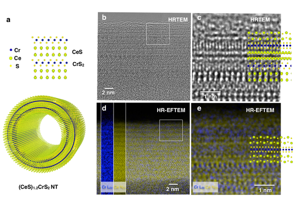
Fig. 2: Atomic-resolution micrographs and spectroscopic images of a CeCrS3 nanotube. (a) Schematic view of the CeCrS3 misfit lattice and a tubular structure. (b) HRTEM image and (c) magnified region of (b) with crystallographic projections superimposed. (d) EFTEM maps showing alternating Ce and Cr signals and (e) magnified region of (d). |