IT-2-O-2611 The detection of single dopant atoms by high-resolution off-axis electron holography
In 2003, a paper was published that discussed the need for a technique to detect single dopant atoms. It was stated that “single dopant atom detection is critical to device design, but it can also unravel complex and unexpected phenomena which may also open up new areas of materials exploration”. In 2014, it is still highly challenging to measure the locations, chemical identities and electrostatic potentials of single dopant atoms [1].
The technique of off-axis electron holography in the transmission electron microscope (TEM) involves the use of an electron biprism to interfere an electron wave that has passed through a thin specimen with a reference wave, in order to form an interference pattern that can be used to determine the phase shift of the electrons. Although electron holography has been used for many years to measure dopant potentials in semiconductors, soon devices will become so small that measurements of the electrostatic potentials of individual dopant atoms may be required.
Based on simulations, the expected step in phase shift across a single ionized P atom in Si is ~2π/1000 radians. This level of sensitivity can be reached easily in electron holographic measurements at low spatial resolution if long acquisition times are used. However, it is more of a challenge at atomic resolution. Here, we demonstrate progress towards the detection of single dopant atoms using electron holography. Figure 1(a) shows an electron hologram acquired at 80 kV using an aberration-corrected FEI Titan Ultimate TEM equipped with a high brightness gun, a monochromator and a single biprism. A careful choice of microscope lens settings allows holograms to be acquired with excellent interference fringe contrast and fine fringe spacing. Figure 1(b) shows an intensity profile extracted from the hologram, while Fig. 1(c) shows the experimentally measured phase resolution plotted as a function of interference fringe spacing, demonstrating that the conditions required to detect single dopant atoms are within reach if large numbers of phase images are added together.
Figure 2(a) shows part of an off-axis electron hologram of a thin MoS2 crystal recorded using an interference fringe spacing of 40 pm. The corresponding reconstructed phase image in Fig. 2(b) has a spatial resolution of 0.12 nm, while the line profile in Fig. 2(c) demonstrates that individual atomic columns with a spacing of 0.12 nm can be resolved. We are presently working towards the acquisition of signals from single dopant atoms in graphene and silicon and comparing our results with scanning TEM images. Great care is required to optimize specimen preparation and to minimize radiation damage, electron beam induced charging and contamination.
[1] Castell et al. Nature Materials 2, 129-131 (2003)
DC and RDB thank the ERC for the starting grant “Holoview” and the advanced grant “IMAGINE” respectively.
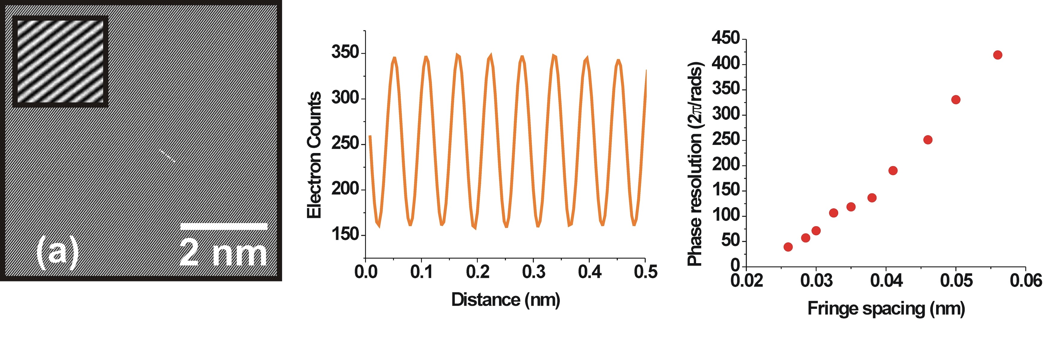
Fig. 1: (a) An off axis electron hologram acquired with a fringe spacing of 50 pm (b) profile of the fringe intensity showing a contrast of 33 %. (c) Experimentally measured phase resolution as a function of fringe spacing (spatial resolution is 2-3 times the fringe spacing). |
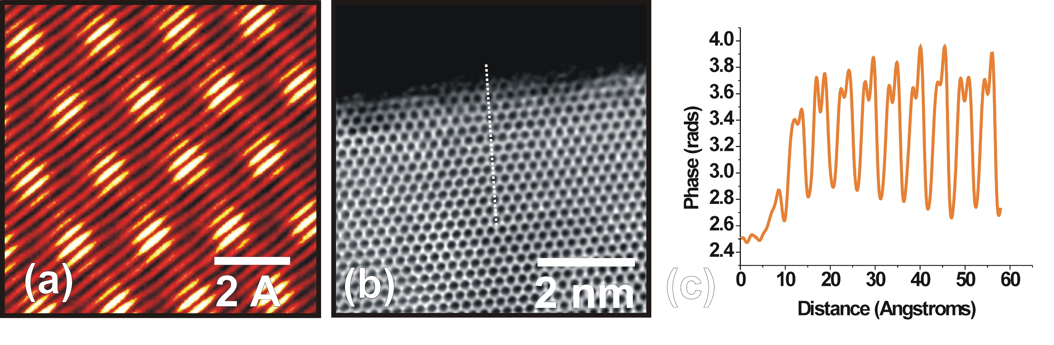
Fig. 2: (a) Detail of an off-axis electron hologram of a MoS2 crystal with a fringe spacing of 40 pm (b) reconstructed map of the electrostatic potential profile and (c) profile showing that the 1.2 A spaced atoms have been resolved. |