IT-13-P-2590 Enabling future Nanotomography and Nanofabrication with Crossbeam technology
A Focused Ion Beam (FIB) combined in one instrument with a Field Emission Scanning Electron Microscope (FE-SEM) has become a powerful instrument for numerous Standard and cutting edge applications in Research and Industry. The FIB is mainly used to open up the third dimension to a SEM. The ion beam is not only able to cut slices of a samples surface for tomographic imaging, but can also be used to create new materials or functional structures with superior properties. With increasing application maturity also the demand for faster systems, complete detection, more precise structuring and a wider application range rises.
3D-imaging and –analytics allow a complete characterization of a samples volume. It is widely used in Materials and Life Sciences and allows better understanding of compound materials, brain tissues, electronic devices and other samples. To achieve representative information of a sample, the analyzed volume needs to be sufficiently large and the resolution has to be high. The voxel resolution in tomography is mainly limited by the thickness of the slices cut with the ion beam [1]. The Crossbeam 540 allows the thinnest slices down to 5 nm and below. To keep the thickness homogenous over thousands of slices, a long-term stable FIB comes along with a sophisticated Software solution including adaptive slice thickness tracking (Figure 1). In interaction with a charged particle beam, each material behaves different. We introduce solutions to process, image and analyze all kinds of samples, including charging, outgassing or dirty and even magnetic samples. We will discuss our latest developments in detector technology to improve the signals especially at low acceleration voltages and the acquisition time.
Preparation of samples for TEM or other imaging techniques is one of the main applications for modern FIB-SEM instruments. Not only the quality, thickness and homogeneity of the prepared specimen matters, but also an fast, easy and integrated workflow. The quality of the results in TEM and STEM depend not only on the instrument, but to a high degree on the analyzed specimen. The unique X² method combined with a FIB that performs excellently at low voltages provides homogenous TEM lamellas with < 10nm thickness and minimum amorphous layer [2] (Figure 2).
Modern FIB-SEM systems cover not only the typical application range but are also used to host and integrate numerous instruments and components for advanced experiments. The Zeiss FIB-SEM allows integration of many components for In-Situ analysis like heating, cooling and tensile stages, SIMS, EBIC and CL, different manipulators, e.g. for probing and liftout, a Laser option for micropatterning or fast removal of large amounts of material and many more.
[1] L. Holzer and M. Cantoni, Review of FIB-tomography, Nanofabrication Using Focused Ion and Electron Beams: Principles and Applications (2011), p. 410ff
[2] L. Lechner, J. Biskupek and U. Kaiser, Improved Focused Ion Beam Target Preparation of (S)TEM Specimen - A Method for Obtaining Ultrathin Lamellae, Microscopy and Microanalysis 18 (2012), p. 379-384
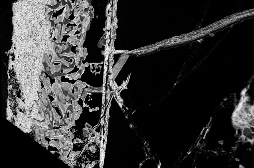
Fig. 1: Innovative thermo-electrical generator transforming exhaust heat into electrical power (Mg2Sn-Mg2Si). 3D stack was acquired on Crossbeam running ATLAS3D. 8nm Voxel Size. The diffusion zone thickness varies between 10 to 25µm |
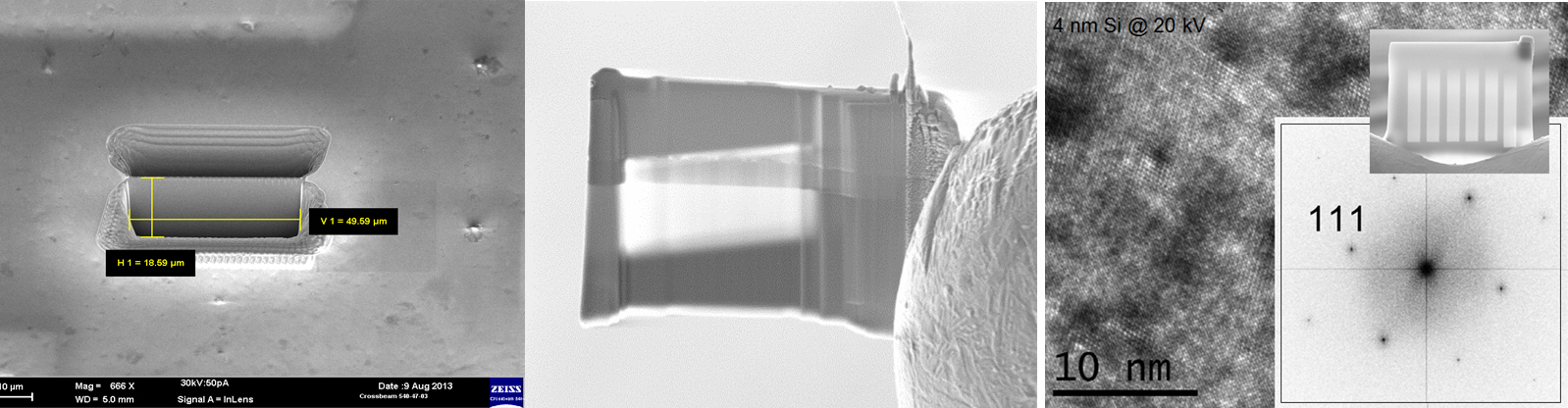
Fig. 2: large 50µm x 20µm TEM lamella prepared automatically in 25 min (left). Lamella thinned using the X²-method (centre). HRTEM image of a lamella demonstrating atomic resolution at 20kV. The spotty contrast variations in the image are caused by strong dynamic diffraction contrast that cannot be avoided at 20 kV [2] (right). |