IT-1-P-2578 Design of a monochromator for aberration-corrected low-voltage (S)TEM
Low-voltage analytical electron microscope equipped with delta-type aberration correctors for image- and probe-forming lens system [1] was developed under a project “Triple-C phase-1” to study the atomic structures of carbon materials sensitive to the damage by irradiation of electrons. It enabled us to reveal the characters of graphenes by EELS [2] and to visualize and specify an encapsulated single metal atom in a fullerene [3]. However this microscope was equipped with a cold field emission gun to obtain high brightness therefore its energy resolution remains at approximately 0.3 eV.
For the next challenges, we have started to develop a new type of low-voltage aberration-corrected analytical electron microscope equipped with a monochromator working at 15-60 kV under a project “Triple-C phase-2”, whose targeted energy resolution is better than 25 meV. Fig. 1(a) and 1(b) show an appearance of the microscope and a configuration of components inside the cover.
The developed monochromator employs a double Wien-filter system, arranged between the extraction anode of Schottky source and the accelerator, which is similar configuration to previous design [4]. The electron trajectories from the electron source to the plane of the exit crossover of the monochromator are calculated as shown in Fig. 2. Electron trajectories are set to be symmetric to the plane of energy-selection slit so that the energy-dispersion formed by the first Wien-filter at a slit plane is cancelled by the second Wien-filter at an exit plane as a consequence of the double Wien-filter system. Thus, after the monochromator, the electron probe is achromatic and the energy spread is controllable by choosing the width of the slit, independently on the probe size. In addition, the setting of the monochromator and the electron trajectories inside the monochromator are independent of the change of the accelerating voltage since the accelerator of the electron gun is located after the monochromator and the potential along the optical axis inside the monochromator is kept constant.
We intend to evaluate the performances of the developed low-voltage monochromated electron optical system and the enhancement of spatial resolution arising from a small chromatic aberration in TEM at low accelerating voltage with large scattering cross-section and small specimen damage by reducing a primary electron energy.
References
[1] H. Sawada, et al.: J. Electron. Microsc. 58 (2009) 341.
[2] K. Suenaga and M. Koshino, Nature 468 (2010) 1088.
[3] K. Suenaga, et al.: Nature chemistry 1 (2009) 415.
[4] M. Mukai, et al.: Ultramicroscopy (2014) accepted.
This work is supported by Japan Science and Technology agency, Research Acceleration Program.
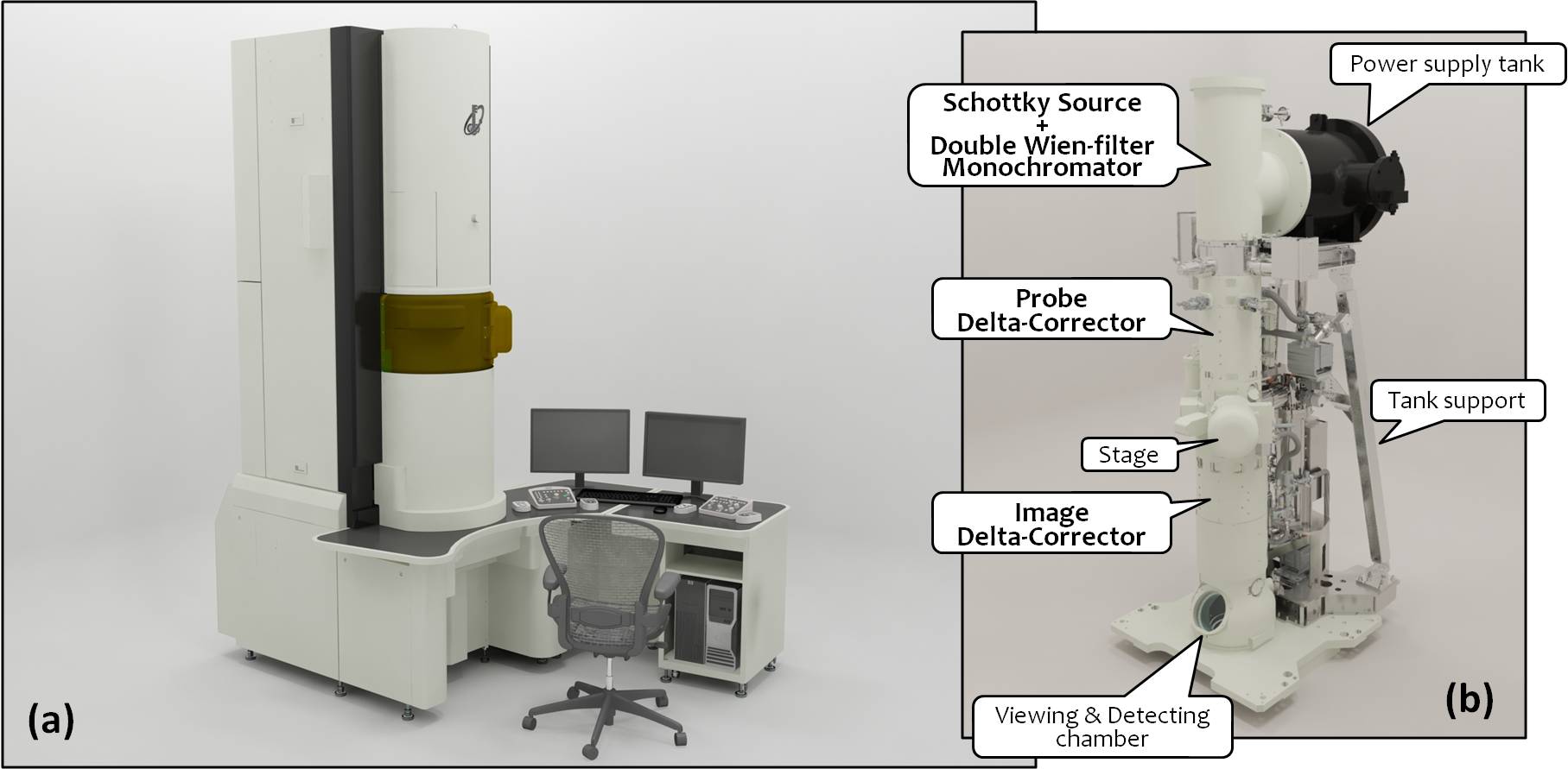
Fig. 1: Computer graphics of a low-voltage aberration-corrected analytical electron microscope equipped with the developed monochromator, (a) An appearance with the cover and (b) a column of the microscope inside the cover. |
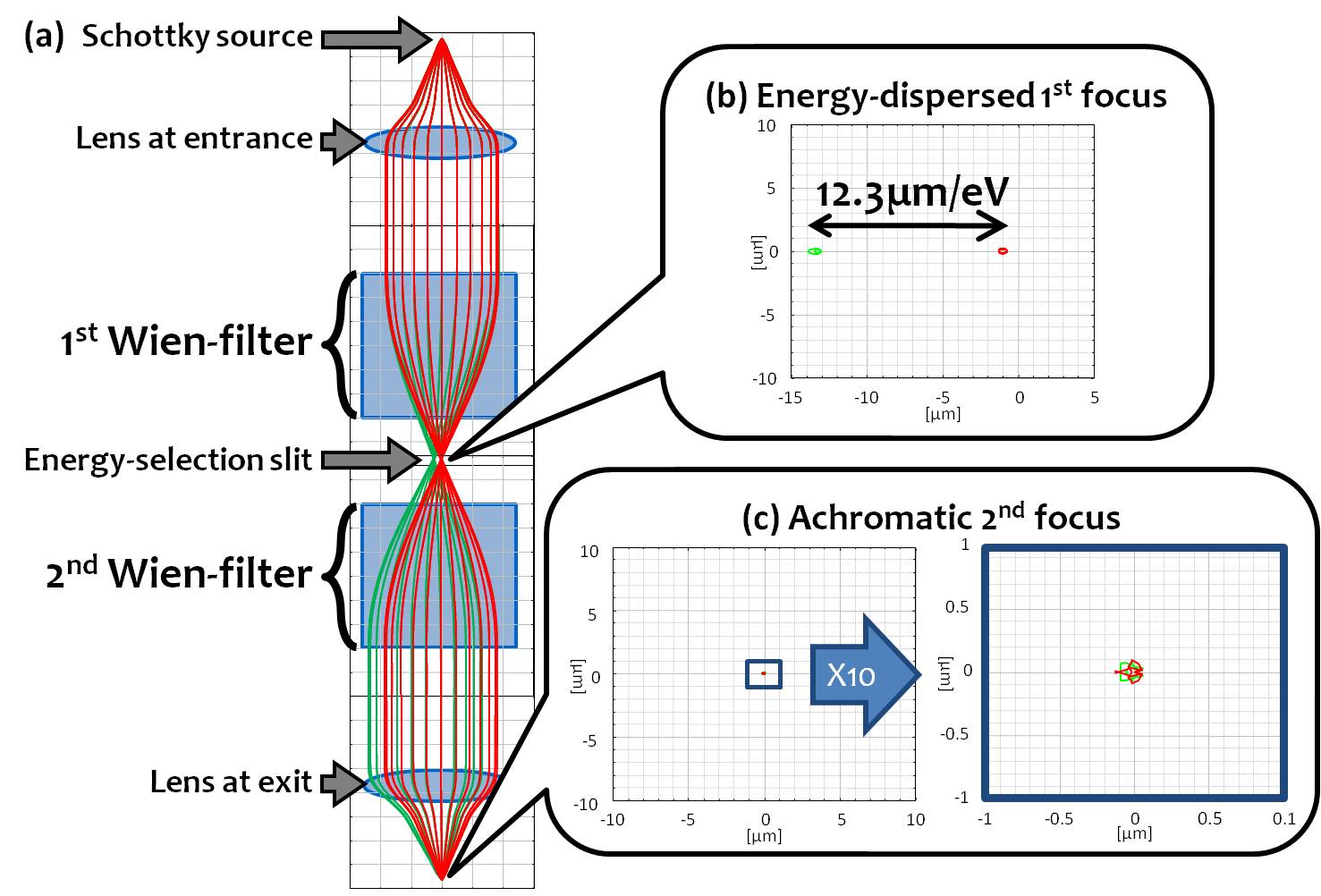
Fig. 2: (a) Calculated trajectories along optical axis from source to exit of monochromator, (b) beam shapes at slit plane with an energy-dispersed 1st focus and (c) beam shapes at exit plane with an achromatic 2nd focus. The red lines and the green lines show the trajectories having different energies of 1 eV inside of the monochromator. |