IT-2-IN-2576 Insights into Materials Properties with Quantitative STEM and EELS
The development of aberration correctors in scanning transmission electron microscopy (STEM) has dramatically improved the analytical “toolkit” of materials scientists. In particular, when combined with electron energy loss spectroscopy (EELS), STEM makes it possible to detect compositional and spectroscopic changes at the atomic level that can be used to understand the structure, and ultimately the performance of materials. Here we present some examples of quantitative STEM and EELS as applied to the study of graphene-based materials, complex nanoparticles used in electrocatalysts, and the defects generated in implanted Si and plasmonic structures.
An FEI Titan microscope was used for this work. With this system, we imaged Pt atoms on multilayer graphene nanosheets (GNS) and demonstrate that single Pt atoms are stabilized during atomic layer deposition on N-doped GNS. Quantitative analyses of images show that the single atoms are located at GNS edge steps and that the doping strongly suppresses the growth of Pt clusters (Figure 1a, b) [1]. Similarly, quantitative images have been used to detect atomic displacements on PtFe intermetallic core-shell nanoparticles that exhibit very high specific activity compared to pure Pt [2,3]. Not only is elemental mapping at the atomic scale possible, but the high beam current and fast spectrometers also allow the acquisition of maps with large sampling of the nanostructure. This is illustrated in the study of PtRu nanocatalysts used in fuel cells where Ru core-Pt shell structures are very clearly mapped (Figure 1c).
Beyond the “simple” deduction of the distribution of elements in nanostructures from maps, quantification is essential to understand the detailed structure of defects and correlate compositional measurement with the optical response of materials. The detailed quantification of the atomic position of a defect, in this case a so-called {311} defect [4] generated by the implantation of ions in Si [4,5] shows that an excellent agreement is obtained between the experimental atomic positions and molecular dynamics simulations (Figure 3) [4] with an accuracy of better than 0.05nm for more than 100 atomic columns. Similarly, quantitative analysis of SiGe alloys has allowed us to deduce compositional fluctuations and interdiffusion in proximity of interfaces [6].
[1] S. Stambula et al., J. Phys. Chem. C, on-line (2014), DOI: 10.1021/jp408979h
[2] S. Prabhudev et al., ACS Nano 7, 6103-6110, (2013)
[3] M.C.Y. Chan et al, Nanoscale 4 (22), 7273-7279, (2012)
[4] K.J. Dudeck et al., Physical Review Letters, 110, 166102 (2013)
[5] K.J. Dudeck et al., Semiconductor Science and Technology, 28, 125012, (2013)
[6] G. Radtke et al., Physical Review B 87, 205309, (2013)
The authors are grateful to NSERC for supporting this research. The microscopy was carried out at the Canadian Centre for Electron Microscopy, a National facility supported by NSERC and McMaster. We are grateful to Paolo Longo (Gatan Inc.) for the help in setting up the Quantum 966 spectrometer.
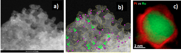
Fig. 1: HAADF STEM image of single Pt atoms and clusters stabilized on N-doped GNS. Raw signals (a), edges and atoms detected (b). Green arrows point to the few Pt atoms (pink) stabilized on GNS terraces (edges labeled in yellow) [1]. (c) elemental maps of PtRu core-shell nanoparticles |
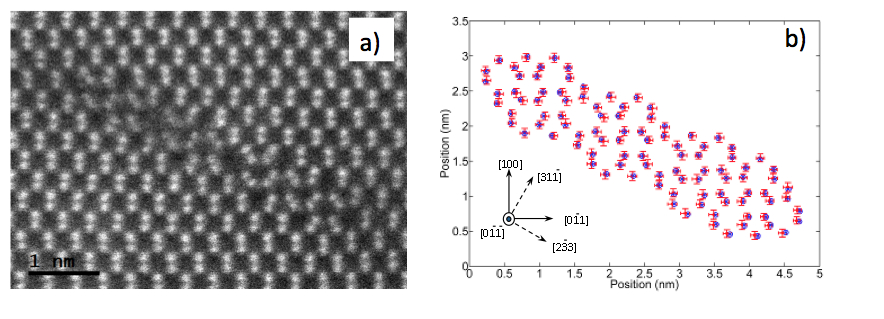
Fig. 2: HAADF STEM image of a {311} defect in Si (a) and the deduced atomic positions (crosses) in (b) with the expected atomic positions deduced by molecular dynamics calculations [4]. |