IT-10-P-2565 Using transmission electron tomography to unravel the structure of hybrid active layers in non volatile memory elements
The interest in plastic electronics has grown significantly over the last twenty years with the development of new electronic devices, particularly solar cells and field effect transistors. More recently, non-volatile memories (NVMEM) based on hybrid materials gained particular interest [1,2]. Typically such devices consist of an insulating or semi-conducting layer sandwiched between a bottom ITO electrode and an upper metallic electrode (silver or aluminum). Bias application on these devices switches them from a low current OFF state to an ON state at high current. The switching mechanism involves the formation of "conducting filaments" [3] in the active layer but no direct observation of such filaments in a hybrid device was demonstrated so far. In hybrid layers, the formation of filaments is eased by the presence of metallic nanoparticles. It is therefore important to understand how such nanoparticles are dispersed in a polymeric matrix. In this study, we have analyzed the morphology of hybrid layers of polystyrene loaded with functionalized Au nanoparticles (NPs). TEM tomography allows to determine the 3D distribution of the nanoparticles in the devices. Evidence is found for the formation of large clusters of Au NPs that are rejected to the top surface of the active layer during the film spin-coating. Moreover, a fraction of Au NPs is dispersed in the PS film but only within an interfacial layer close to the bottom ITO substrate whereas the largest part of the PS matrix does not contain any Au NPs. It is shown that TEM tomography is a valuable tool to unravel the 3D structure of the active layers in NVMEM.
[1] J.C. Scott et al., Adv. Mater. 2007, 19, 1452.
[2] B. Cho et al., Adv. Funct. Mater. 2011, 21, 2806.
[3] S. Nau et al., Adv. Mater. 2014, DOI: 10.1002/adma.201305369.
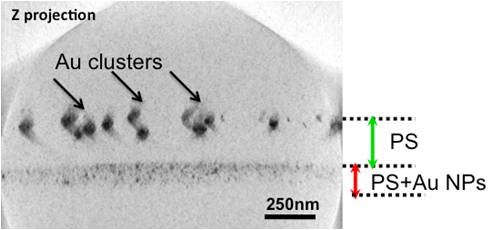
Fig. 1: Cross-sectional view of the active layer of a hybrid non volatile memory element obtained by tomography. The active layer is made of a polystyrene matrix loaded with Au nanoparticles. |