IT-14-P-2536 Surface potential investigation of AlGaAs/GaAs heterostructures by Kelvin Force Microscopy
The Kelvin force microscopy (KFM) provides a spatially resolved measurement of the surface potential, which is related to the energetic band structure of a material. The goal of this work is to investigate the surface potential measured by KFM on AlGaAs/GaAs heterostructures.
For this study, we selected a certified reference sample BAM-L200 [1] composed of epitaxial layers of AlGaAs and GaAs, with a decreasing thickness (600 to 2 nm) and an uniform Si (n) doping (5.1017 cm-3). The surface potential measurement is performed with an Omicron XA VT AFM, under ultra-high vacuum (of 10-11 mbar). Two scanning modes are used: the amplitude modulation (AM-KFM), sensitive to the electrostatic force and the frequency modulation (FM-KFM), sensitive to its gradient. [2] Three kinds of tips have been used for this study: Platinum coated silicon tips (BudgetSensors), Au nanoparticles coated silicon tips (Next Tip) and super sharp silicon tips (Nanosensors).
We will present the measurements obtained with these different tips on the sample area containing the narrowest layers. The relevant result is the fact that the contrast decreases with diminution of the layer thickness. With Pt-coated Si tips, a maximum contrast of about 270 meV was observed, whereas for super sharp Si tips the maximum contrast equals 290 meV [Fig. 1]. This contrast vanishes when layer thickness becomes thinner than 5 nm for Pt-coated SI tips and 3 nm for super sharp Si tips. This loss of contrast can be explained primarily by the resolution limit of our instrument but also the band bending length scale at the AlGaAs/GaAs interface, related to the dopant concentration. The contribution of band bending between the layers to the measured potential is evaluated by a self-consistent simulation of the electrostatic potential, accounting for the free carriers distribution inside the sample and for the surface and interface dipoles. As shown in Fig. 2, the electric fields of the narrow layers recover each other, resulting in the partial or total loss of the intrinsic sample structure. Simple comparison of simulation with KFM surface potential measurements provides information that KFM measurements represent real values and are not influenced by KFM resolution limit.
All measurements were made on the CEA Grenoble nanocharacterization platform (PFNC).
[1] M. Senoner, T. Wirth, W. Unger, W. Österle, I. Kaiander, R. L. Sellin and D. Bimberg, BAM-L002 - a new type of certified reference material for length calibration and testing of lateral resolution in the nanometre range, Surface and Interface Analysis 36, 1423-1426 (2004)
[2] S. Sadewasser and T. Glatzel, Kelvin Probe Force Microscopy (2012)
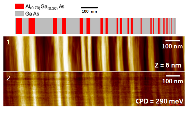
Fig. 1: KFM images obtained on BAM-L200 with super sharp silicon tips, with respect to sample schema: (1) Topographic image; (2) Surface potential images. |
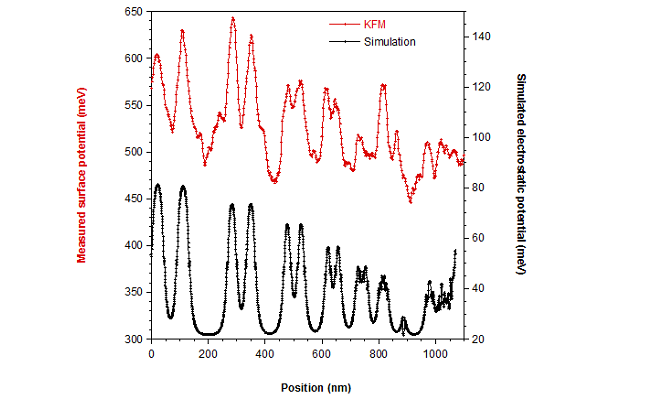
Fig. 2: Theoretical simulation of the electric potential at 5 nm above the surface of the sample, and averaged section of previous KFM image. |