IT-11-O-2513 Observation of electric field using electron diffractive imaging
Information on electromagnetic fields in and around nanometer-sized semiconducting or magnetic devices is obtained from phase shifts of illumination electron waves. Although the most established method for phase imaging is presently off-axis electron holography, another choice could be electron diffractive imaging (EDI). In the method, a complex wave field is reconstructed from a diffraction pattern through numerical iterations under some constraints in real space. So far we have succeeded in reconstructions of atomic structures of crystals [1, 2] and thickness maps of wedge-shaped Si [3]. Figure 1 shows an example of the results, in which phase image of the transmission electron wave undergoing dynamical diffractions is reconstructed from the primary spot in a selected-area diffraction (SAD) pattern. In the present study, we performed reconstructing electric fields around MgO nano particles and a p-n junction in GaAs.
A 200kV thermal field-emission TEM (JEOL: JEM-2100F) was used for taking SAD patterns with spatially coherent illumination. A post-column energy filter (Gatan: GIF tridium) was utilized for removing inelastic background intensity from samples and also for achieving a camera length large enough for precise sampling of low-angle scattering intensity. Energy-filtered bright field TEM images were also recorded to use as the real-space constraints. Figure 2 shows the phase reconstruction around MgO particles isolating in the vacuum. In Fig. 2(c), the electric field, which radiates from the particles positively charged by electron beam irradiation, is clearly observed. The reconstruction of the p-n junction in GaAs is shown in Fig. 3. Although the junction is invisible in the TEM image (Fig. 3(a)), the potential change deforms the primary spot (Fig. 3(b)), which results in visualization of the junction in the reconstructed phase image (Fig. 3(c)). The width of the depletion layer and the offset across the junction agree well with the doping concentration and measurements by off-axis electron holography.
Unlike off-axis electron holography, the present method needs neither electron biprisms nor a vacuum area adjoining to the field of view of interest. The present study exhibits the future possibility that EDI will become an alternative to electron holography in some cases for observing electromagnetic fields relating to nanometer-sized materials.
References
[1] S. Morishita, et al., Appl. Phys. Lett. 93 (2008) 183103.
[2] S. Morishita, et al., AMTC Lett. 2 (2010) 116.
[3] J. Yamasaki, et al., Appl. Phys. Lett. 101 (2012) 234105.
We thank Dr. S. Morishita in JEOL Ltd. for valuable discussions. The present study was partly supported by JSPS KAKENHI (Grant No. 21760026), The Public Foundation of Chubu Science and Technology Center, and Toyoaki Scholarship Foundation.
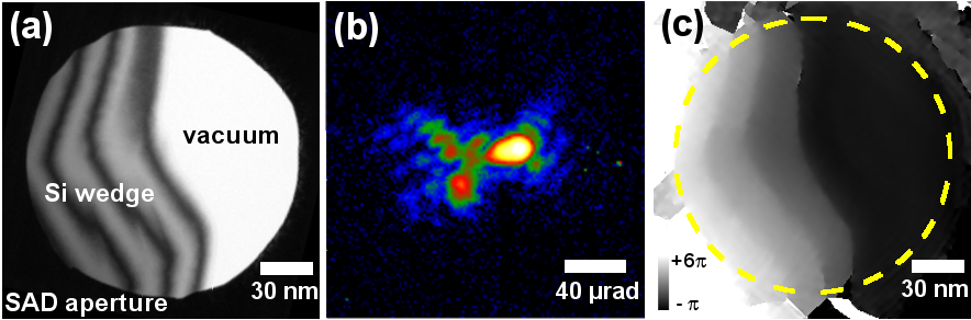
Fig. 1: Reconstruction of the phase image of the wedge-shaped Si crystal by electron diffractive imaging. (a) Bright-field TEM image, (b) the primary spot in the SAD pattern, and (c) the reconstructed phase image. |
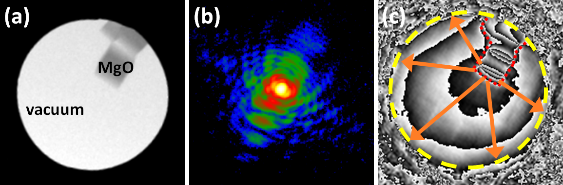
Fig. 2: Visualization of electric field (arrows) around the charged MgO particles. (a) Bright-field TEM image, (b) the primary spot, and (c) the phase image. |
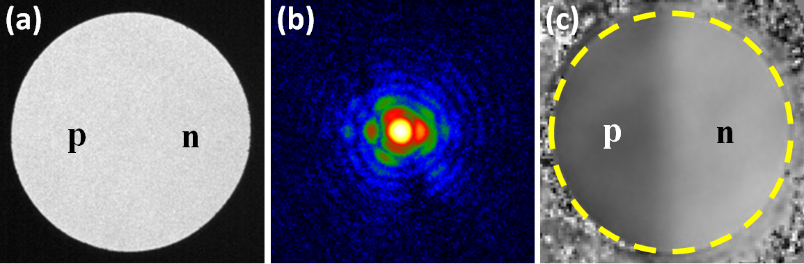
Fig. 3: Visualization of the p-n junction in GaAs. (a) Bright-field TEM image, (b) the primary spot, and (c) the phase image. |
|